List of Illustrations
Figure Number Page Figure Page
............
3.1
.
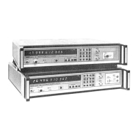
Front Panel. Model 545A
............
3-1 01.1
.
DAC Board. Simplified 01-2
.
................
............
3.2
.
Front Panel. Model 548A 3-3 01.2 Key board Control 01-4
.
...............
......................
3.3
.
Rearpanel 3-4 01.3 DAC Board Update 01-5
.........
.
......................
3.4
.
Keyboard 3-5 01.4 DAC Component Locator 01-10
01.5
.
DAC Schematic
................
01 -1 1
4.1
.
Counter Block Diagram, Simplified
.....
4-1
Band 2 Converter Block Diagram.
Simplified 4-3
02.1
.
.....................
Band 2 Converter Operation 4-4
02.2
.
..........
Band 2 Operating Ranges 4-5
02.3
.
............
Band 3 Converter, Simplified
.........
4-6
Band 3 Operation. Simplified 4-8
02.4
.
.........
Band 3 Search for Signal
...........
4-10
Determine Largest Signal
...........
4-1 1
YIG Centering
..................
4-1 2
Calculate
N
and VCO Frequency
......
4-13
Band 3 Signal Tracking
............
4-14
Increase VCO Reference Frequency
....
4-1
5
Band 4 Overall Operation
...........
4-16
Harmonic Mixing Ranges
...........
4-1 7
Search for Signal
................
4-18
Center YIG on Signal
.............
4-1 9
Determine
N
and
+I-
Sign
..........
4-20
Select Proper VCO Frequency
........
4-21
Microprocessor Free Running Signatures
.
.
6-2
Basic PROM Set
..................
6-3
Self Diagnostic Error Indications
.......
6-3
Keyboard Configuration for Tests Requiring
Hexadecimal Inputs
..............
6-4
Keyboard Test Signatures
............
6-5
Converter Ramp Test Signatures
.......
6-6
I10
Addresses
..................
6-8
RAM Frequency Storage
...........
6-10
RAM Power Storage
..............
6-10
Troubleshooting Test Equip
.
Required
. .
6-1 1
Main Troubleshooting Tree
..........
6-1 2
Program Inoperative
..............
6-13
Key board
.....................
6-1 4
Band 1
.......................
6-15
200 MHz Test
..................
6-16
Band 2
.......................
6-1 6
Band 3
.......................
6-1 7
Power Meter
&
Power Meter Zero DAC
. .
6-20
Power Meter Hardware
............
02-2
Power Meter Task
................
02-3
Power MeterIGate Generator
Component Locator
.............
02-8
Power
MeterIGate Generator
Schematic
....................
02-9
031415.1
.
Time Base Oscillator Option
Specifications
..............
031415-1
031415.2
.
Component Location. Time Base
...................
Option 031415-2
031415.3
.
Time Base Option, Interconnection
Diagram
..................
031415-2
031415.4
.
Oven Oscillator Power Supply (A1 12)
Component Location
.........
031415-3
.
..........
031415.5 Time Base Calibration 031415-4
.....
.
031415.6 Time Base Option Schematic 031415-6
06.1
.
Frequency Extension Block Diagram
...
06-2
06.2
.
Down Conversion of Band 4 Signal
....
06-3
06.3
.
Band 4 Program, Flow Diagram
.......
06-4
06.4
.
Harmonic Mixing Ranges
...........
06-6
06.5
.
Location of Installed Band 4
Converter
....................
06-8
07.1
.
Data Entry Timing
...............
07-4
07.2
.
Remote ProgrammingIBCD Block
Diagram
.....................
07-7
07.3
.
Remote ProgrammingIBCD Component
Locator
....................
07-10
07.4
.
Remote ProgrammingIBCD
Schematic
...................
07-1 1
08-1
.
Allowable Address Codes
..........
08-1 3
08.2
.
Location of GPlB in Counter
.......
08-14
08.3
.
GPlB Component Locator
.........
08-1 6
08.4
.
GPlB Schematic
................
08-17
010.1
.
Side View of Counter with Option 10
Installed
....................
010-1
Scans by ArtekMedia © 2007