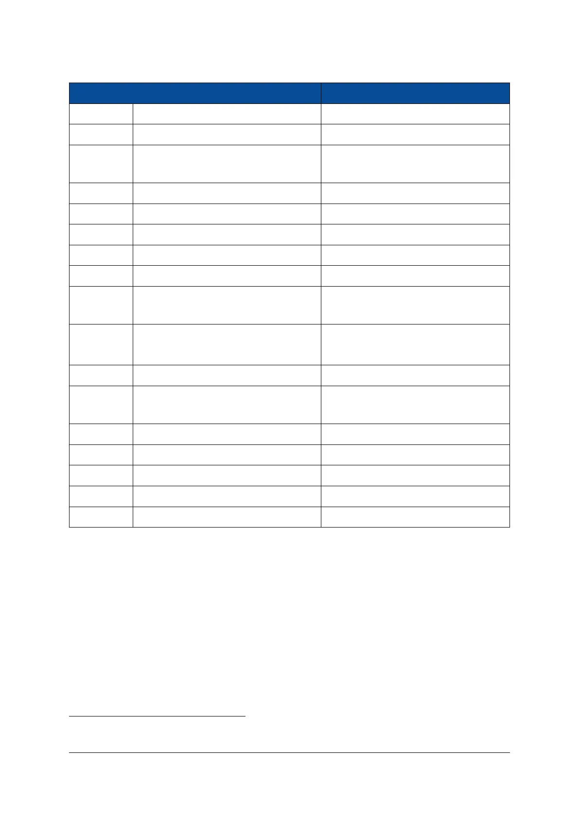
MIO Group Function Connection
0-5 QSPI flash QSPI flash
6 QSPI feedback clock -
10-11 I2C On-board I2C bus and module connector
via level shifter
12 I2C interrupt On-board I2C bus
13-22 eMMC flash eMMC flash
24-25 LED0#, LED1# On-board LEDs
7-9, 23 Unused -
26-29, 31-37 Ethernet Gigabit Ethernet PHY 0
30 Ethernet/PCIe block PERST# signal Gigabit Ethernet PHY 0/Module connector
via series resistor
38 UART RX
7
/user functionality
Module connector
39 UART TX
7
/user functionality
40-41 User functionality Module connector
42 PCIe block PERST# signal
8
/user functional-
ity
Module connector
43-44 User functionality Module connector
45-51 SD card/user functionality Module connector
52-63 USB USB 2.0 PHY 0
64-75 USB USB 2.0 PHY 1
76-77 Ethernet MDIO Gigabit Ethernet PHY 0
Table 10: MIO Pins Connections Overview
8
2.9.8 Analog Inputs
The Zynq Ultrascale+ MPSoC devices contain a system monitor in the PL and an additional system monitor
block in the PS. These are used to sample analog inputs and to collect information on the internal voltages
and temperatures.
The system monitor block in the PL provides a 10-bit ADC, which supports up to 17 external analog lines (1
dedicated differential input, 16 auxiliary differential inputs). The auxiliary analog lines of the MPSoC device
are available on the module connector; these I/Os have the abbreviation “AD” followed by the ADC channel
in the signal name. The ADC lines are always used differentially; for single-ended applications, the *_N line
7
UART RX is an MPSoC input; UART TX is an MPSoC output.
8
Used for PCIe PERST# connection implementation. Refer to Section 2.9.2 for details.
D-0000-445-001 29 / 64 Version 07, 25.07.2019

 Loading...