A 100 MHz differential clock is available on the module and connected to PS_MGTREFCLK2 pins, to be used
as a reference clock for the USB 3.0 interface. It is also possible to provide another reference clock from the
base board to the MGTPS_REFCLK* pins.
Details on the built-in USB 2.0/3.0 controller and on the usage of the PS GTR lanes are available in the Zynq
UltraScale+ MPSoC Technical Reference Manual [19] and in the Zynq UltraScale+ MPSoC Overview [23].
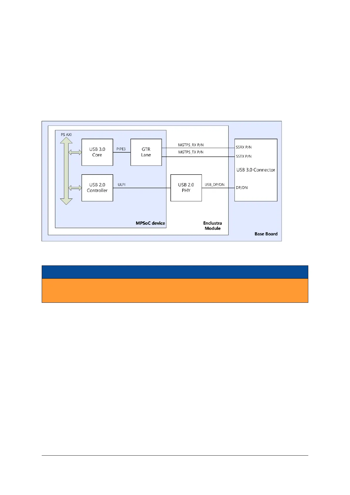
Figure 15 shows an example of a USB 3.0 implementation using the built-in Xilinx USB 3.0 interface and the
USB 2.0 signals from the PHY, all routed to a USB 3.0 connector on the base board.
Figure 15: USB 3.0 Implementation Example
Warning!
The USB 3.0 interface on the Mercury XU5 SoC module uses the GTR lines (MGTPS signals on module
connector B), and not the USB_SSRX_P/N and USB_SSTX_P/N connections on module connector A.
2.24 Display Port
Xilinx Zynq Ultrascale+ devices feature two built-in DisplayPort controllers and PHYs, supporting up to two
lanes at a 5.4 Gbit/sec line rate. Each lane is represented by one of the PS GTR lines, available on the module
connector.
A 27 MHz differential clock is available on the module and connected to PS_MGTREFCLK3 pins, to be used
as a reference clock for the DisplayPort interface. It is also possible to provide another reference clock from
the base board to the MGTPS_REFCLK* pins.
Details on the built-in DisplayPort controller and on the usage of the PS GTR lanes is available in the Zynq
UltraScale+ MPSoC Technical Reference Manual [19] and in the Zynq UltraScale+ MPSoC Overview [23].
D-0000-445-001 47 / 64 Version 07, 25.07.2019

 Loading...