- 39 -
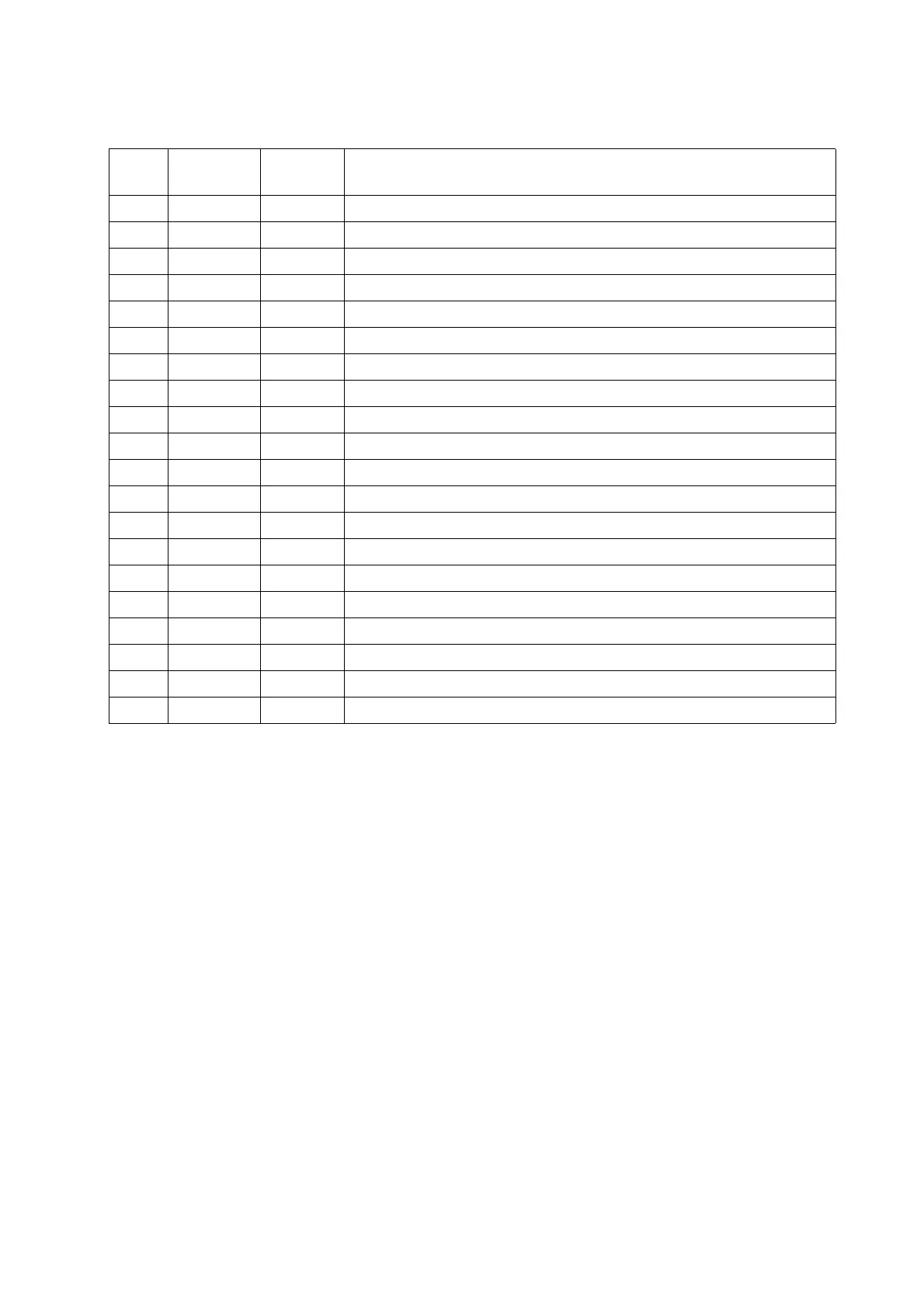
SIGNAL DESCRIPTION OF X2
Inverter supply bus, X7 on A1, X2 on A8
Pin
No.
Signal
Source
Level Description
1 A1 40 V1~ High frequency AC supply for driver stages, line 1
2 A1 40 V2~ High frequency AC supply for driver stages, line 2
3 A1 40 V1~ High frequency AC supply for driver stages, line 1
4 A1 40 V2~ High frequency AC supply for driver stages, line 2
5 A1 40 V1~ High frequency AC supply for driver stages, line 1
6 A1 40 V2~ High frequency AC supply for driver stages, line 2
7 A1 +15 V +15 V supply for control A8
8 A1 -15 V -15 V supply for control A8
9 A8 +15 V Pulse-width modulation for inverter
10 GND GND Logic and supply ground
11 GND GND Not relevant for the DTG 405
12 A2 +15 V Logic and supply ground
13 A1 +15 V Supply error A1, low active
14 A1 +15 V 3-phase mains supply indentification, high active
15 A1 +15 V Error: thermal overload of power stage, low active
16 A1 +15 V Error: primary overcurrent, shut down of power stage, low active
17 A1 +15 V Error: mains overvoltage, low active
18 A1 +15 V Error: mains undervoltage, low active
19 A1 +15 V I>0, low active
20 A1 +5 V +5 V logic supply