TROUBLESHOOTING AND REPAIR
DIGITAL CONTROLLER
Timing PAL U15 adds additional wait states to each module I/O write cycle to ensure
that adequate setup and hold times are provided for every IC on the bus.
Status and Control 6B-10.
Input buffers U35, U36, U37, and U45 read the fault detector signals, hardware status
signals, the option status signals, and the status of the REF INT/EXT and
CAL|COMP switches. Control and buffer enable data is latched by output latches
U34 and
U38.
DIGITAL CONTROLLER TROUBLESHOOTING 6B-11.
If the symptoms indicate a digital or control problem, the following suggestions may
help isolate the fault to a particular functional circuit. Refer to the schematic diagrams
in Section 8.
Verify that all assemblies are receiving the correct voltages from the power supply.
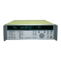
The most obvious symptom of failure in the A13 Controller PCA is a blank front
panel. A properly operating front panel indicates that most of the controller and
display circuitry is functional. If the front panel is totally blank or unresponsive to
keystrokes, make sure that the display blanking special function is not active by
pressing the key or by cycling the power. If the front panel is still blank, refer
to "Microprocessor Kernel" later in Section 6B.
If the front panel is operating correctly but the RF output is incorrect, try to determine
if the fault is on the controller or on an RF circuit board by programming various
functions and checking for status codes.
RF Control 6B-12.
Communication with the RF circuitry in the upper and lower modules is through
connectors J3 and J6 respectively. The RF data and control signals to both modules
are buffered by tri-state drivers that are active only while data is being transferred and
are in the high-impedance state at all other times.
Special Function 903, the latch test, generates continuous activity on the data and
address buses so that the activity can be monitored with an oscilloscope. The latch test
is described under "SOFTWARE DIAGNOSTIC FUNCTIONS" in Section 6.
Enter Special Function 903 to initiate the latch test. Use an oscilloscope to inspect the
chip select signals at the inputs and at the outputs of buffers U24 and U25. The first
symptom to look for is totally inactive signals or invalid logic states. If there are no chip
select signals present at the inputs of U23, refer to "Address Decoding" later in Section
6B.
If all of the chip select signals are operating correctly, connect a scope probe to the
signal BSEL0L and use the high-to-low transition of the signal to trigger the scope. Use
another probe to inspect the data and address signals buffered by U24, U25, U27, and
U33 during the low period of BSEL0L. Look for inactive signals and invalid logic
states. Also compare the buffer inputs to their outputs. Press the STEP key,
then the STEP key to toggle each of the data signals. In addition, make sure
that the buffer control signals are low (active).
6B-4
