TROUBLESHOOTING AND REPAIR
RF LEVEL/AM
With the instrument programmed as in the preceding paragraph, the voltage at TP8
would be +1.3 ±0.5V DC. In the unleveled state, the voltage at TP8 should be greater
than +11V DC. If the instrument is working properly, signal levels between the
modulator and the detector are typically as noted in Table 6D-3.
If the voltage at TP8 is high, the AC voltages will be high unless something is wrong
with this part of the circuitry. Any DC voltage discrepancies should be investigated as
indications of the problem.
If high AC voltages are measured, the unleveled problem is now most likely with the
detector diode, CR20, on the Output PCA or with U7 or U41 and associated circuitry
on the Modulation Control PCA.
Output Assembly Test Point Signal Information 6D-9.
Table 6D-4 presents the nominal characteristics of the signals at the various test points
on the Modulation Control PCA. The table shows the range of the signal and the
expected value for the instrument preset state (SPCL 01).
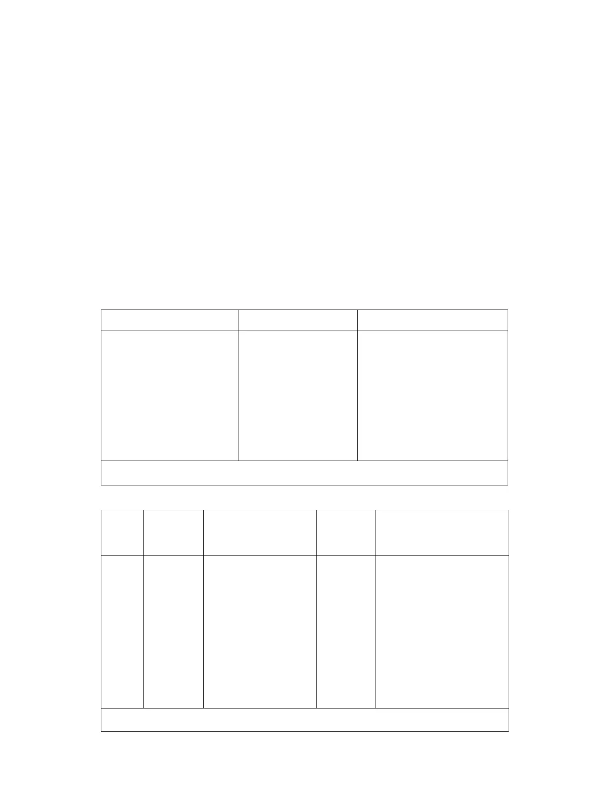
Table 6D-3. Modulator - Detector Nominal Voltages
Table 6D-4. A11 Modulation Control PCA Test Points
6D-9
CR31 cathode
CR28 anode
Q5 collector
U8 output
Q1 collector
CR5 anode
CR14 cathode
CR17 anode
VOLTS DC
-15V
-12V
+7.5V
+5.5V
+9.5V
+.7V
+.7V
+.7V
VOLTS AC @ 88 MHz
180 mV p-p
1.2V
p-p
270 mV p-p
600 mV p-p
1.25V
p-p
1.25V
p-p
1.2V
p-p
1.15V
p-p
NOTE: Measured with a 10 MΩ 8 pF oscilloscope probe with short ground.
TEST
POINT
TP1
TP2
TP3*
TP4
TP5
TP6
TP7
TP8
SIGNAL
TYPE
DC
DC+audio
N/A
Not Used
DC+audio
DC+audio
DC+audio
DC+audio
RANGE
.98 ± 5 mV
+14V
to
0V
.2 to 4V
0 to
2.8V
0.04 to 3.0V DC nominal
+14V dc nominal
TYPICAL
FOR
SPCL 01
.980
mV
2.6V
.3V
(on)
.0V DC
1.0V
DC
1.0V
DC
SIGNAL DESCRIPTION
Ext. AM/FM level indicator
reference.
Detector Linearizer output.
Pulse Modulator to Output
PCB.
AM input scaled by % AM.
Leveling loop control voltage.
Modulator control voltage.
* This test point is an input for factory test of ALC loop.