TROUBLESHOOTING AND REPAIR
FREQUENCY SYNTHESIS
Band control signals CSVCO0H and CSVCO1H are decoded by U3 and Q4-Q8. This
circuit applies bias current only to the selected oscillator transistor. Thus, only one
oscillator is activated per band.
PIN diodes CR7-CR9 connect the active oscillator to a resistive signal splitter (R21,
R22) that drives monolithic 11 dB amplifiers U1 and U2. The +7 dBm output of U1
connects to the A2 Coarse Loop PCA at J7 by a through-the-plate coaxial connector,
and the output of U2, also at +7 dBm, connects to the A12 Sum Loop PCA at J8 by a
coaxial cable.
COARSE LOOP VCO TROUBLESHOOTING 6C-27.
The Coarse Loop VCO PCA, controlled by the Coarse Loop PCA, generates the
coarse loop signal that is further processed in the Sum Loop PCA. A problem with the
Coarse Loop VCO can cause Coarse Loop Unlock status code 243 to appear. Self-test
error codes 320 through 323 can also be triggered by a faulty Sum Loop VCO. To
determine that the Coarse Loop VCO is faulty, rather than another assembly, the
following tests can be performed. First, ground J5, the phase lock port of the VCO with
a clip lead. Next, measure the DC voltage at J6 with the UUT programmed to SPCL
943 (All DACs to full scale). The reading should be 24.00V. Next, program the UUT to
SPCL 942 (All DACs to half scale). The reading should be 12.00V. This tests the VCO
steering voltage circuit.
With J5 still grounded, examine the output at connector J8 with a spectrum analyzer as
frequency is stepped in 8-MHz increments from 512 MHz to 1056 MHz. The frequency
should always be within about 2 MHz of expected coarse loop frequency, and the level
should be approximately +5 dBm. Note that the expected coarse loop frequency can be
displayed by entering SPCL 946. If the signal is good, the problem is likely in another
PCA. If the signal is faulty only over a frequency band corresponding to one of the
VCO bands, the associated VCO circuit is likely at fault. If the VCO appears to be
faulty, DC voltages can be measured at various circuit nodes with the UUT
programmed to frequencies corresponding to the three VCO bands. UUT frequencies
of 600, 700, and 1000 MHz will enable each of the three bands. Refer to Table 6C-7 for
expected approximate voltage measurements. These measurements should help isolate
the faulty circuit.
SUM LOOP BLOCK DIAGRAM 6C-28.
Refer to the Sum Loop Block Diagram (see Figure 6C-8) for help in identifying the
major functional sections and following the signal paths of the sum loop.
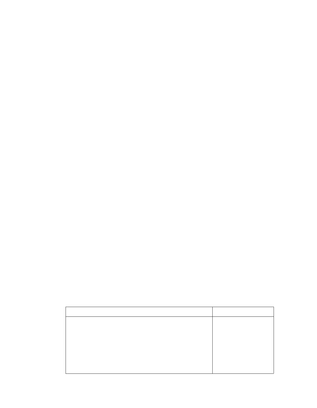
Table 6C-7. A5 Coarse Loop VCO PCA Expected DC Voltages
LOCATION
ON bias transistor collector (Q4, Q5, or Q6, depends on band)
OFF bias transistor collectors
ON oscillator transistor collector (Q1, Q2 or Q3, depends on band)
OFF oscillator transistor collectors
U1, U2 outputs
CR7, CR8, CR9 node
VOLTS DC
-14.3
0
+8.3
+9.6
+4.4
+9.9
6C-32