TROUBLESHOOTING AND REPAIR
FREQUENCY SYNTHESIS
PROCEDURE:
The output of the Discriminator Video Amplifier (TP9) is adjusted to 0V DC.
1. Program the UUT to SPCL 909.
2. Connect the DVM to measure voltage between TP9 and ground.
3. Adjust R102 for 0V ± 10 mV.
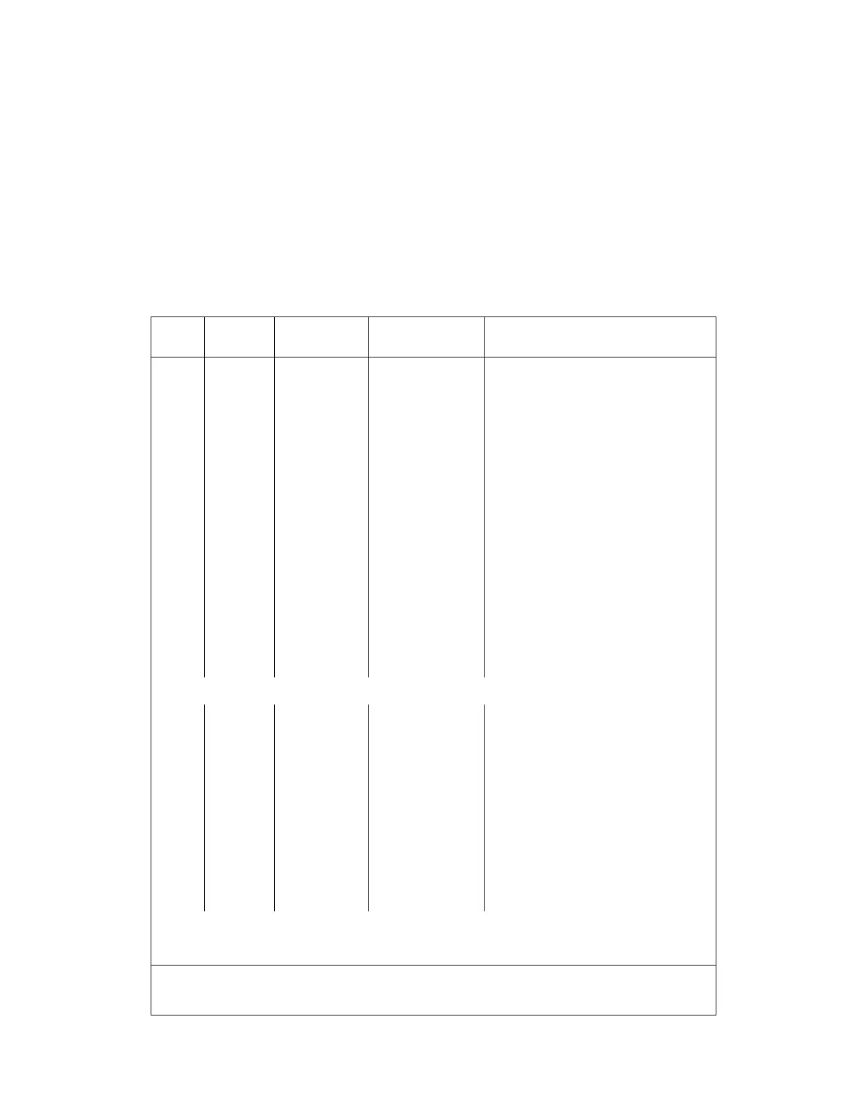
Table 6C-6. A2 Coarse Loop PCA Test Points
TEST
POINT
TP1
TP2
TP3
TP4
TP5
TP6
TP7
TP8
TP9
TP10
TP11
TP12
SIGNAL
TYPE
ECL
ECL
RF-ECL
AC
AC
DC
DC
DC
DC
DC
Ground
RANGE
40 MHz
0-16
MHz
120-240 MHz
40 MHz
40 MHz
± 1V
±
0.1V
2-22V
±50 mV
±50 mV
TYPICAL
800 mV p-p
2 MHz 25 ns AH
162 MHz, +5 dBm*
1V p-p
1.2V
p-p
Varies
Varies
11V
Varies
Varies
SIGNAL DESCRIPTION
N-divider Output
Rate Multiplier Output
Divide-by-4 Prescaler Output
40 MHz Oscillator Output
40 MHz Reference Amplifier Output
Loop Amplifier/Acquisition Oscillator
Output
VCO Phase-Lock Port
VCO Steering Port
Discriminator Loop Amplifier Output
Input for test
Low-Pass Filter Output
TP13 Shorting connection to disable acquisition oscillator
TP14
TP15
TP16
TP17
TP18
TP19
Ground
TTL
AC
AC
DC
DC
10 MHz
20 MHz
40 MHz
12.7
±
0.2V
0.8 ±
0.2V
1-11V
150ns AL
1V p-p
800 mV p-p
Constant
Constant
5.6V
Reference Loop Phase Detector Output
20 MHz Reference to Modulation
Oscillator
40 MHz Reference to Sub-Synthesizer
On when internal TXCO
Off when external or high/medium
stability option
Reference Loop Amplifier Output
TP20 Shorting connection to open reference loop for troubleshooting
TP21
* As measured with 500 ohm 10X RF probe (TEK 6156). Actual level as displayed on spectrum
analyzer will be approximately 20 dB lower.
6C-27