TROUBLESHOOTING AND REPAIR
FREQUENCY SYNTHESIS
If the above signals are at the correct frequency and level, the problem is likely in the
sum loop or the Sum Loop VCO. The Sum Loop VCO can be checked for proper
operation by shorting to ground TP4, the phase lock port, and measuring the Sum
Loop VCO signal at TP12 using a 500-ohm probe with a spectrum analyzer. The
measured frequency should be within 2 MHz of the expected sum loop frequency. If
the signal is absent or is far off frequency, either the sum loop VCO or the VCO steering
voltage circuit is faulty. The steering voltage circuit can be checked by programming
the UUT with SPCL 943, and measuring the DC voltage at TP3, the VCO steering
port. This special function programs the steering DAC to full scale, and should result
in a reading of 26.00V. If the Sum Loop VCO seems to function properly, the Sum
Loop PCA is probably faulty.
With phase lock port TP4 still shorted to ground, use an oscilloscope to measure the
signal at TP5, the phase detector output. This signal should be a triangle wave of about
0.56V peak-peak amplitude. The frequency should be less than 2 MHz. An improper
signal here indicates a problem in the phase detector or the RF circuitry that precedes
it. The RF circuits can be checked and any problem isolated by measuring signal levels
and frequencies at various points with a 500-ohm probe and a spectrum analyzer. Table
6C-9 contains expected frequencies and approximate levels in a suggested test
sequence to aid in troubleshooting. Note that TP4 is assumed to be shorted to ground.
Note also that the 500-ohm probe should be grounded as closely as possible to each test
point. PCA hold down screws and the walls of the plate provide good grounds. As
another aid to troubleshooting, Table 6C-10 contains DC bias voltage information for
circuits in the RF section.
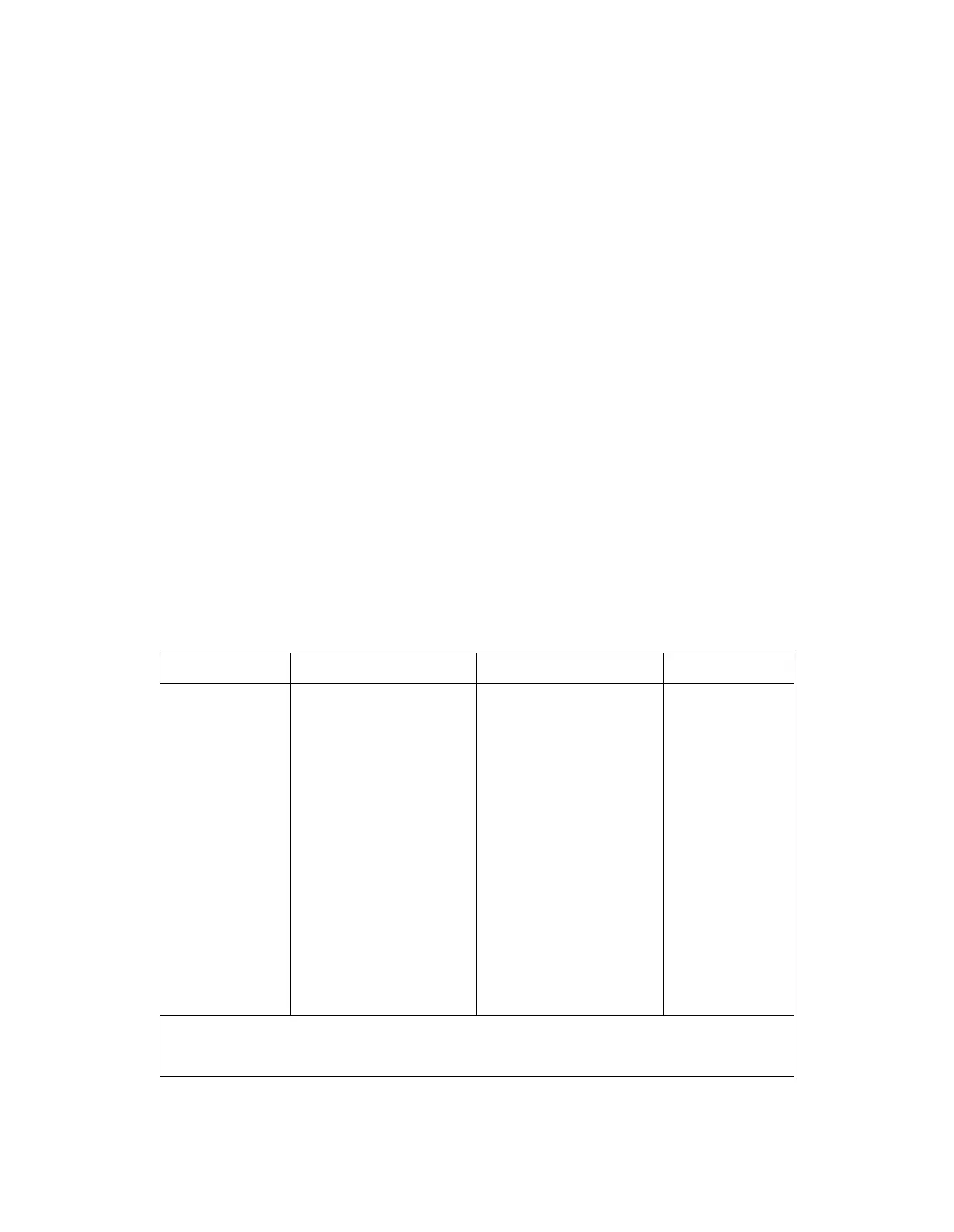
Table 6C-9. A12 Sum Loop PCA RF Circuitry Test Information
LOCATION
J11
TP13
J9
TP12
Q5 base
R25/R26 node
Q6 collector
R17/R45 node
TP14
Q9 base
Q10 collector
J10
R57/C60 node
CIRCUIT
U1 LO amplifier
U1 LO amplifier
U1 RF amplifier
U1 RF amplifier
IF1 amplifier
IF1 amplifier
IF1 amplifier
FM amplifier
FM amplifier
IF2 amplifier
IF2 amplifier
ECL/TTL buffer
U3 LO driver
FREQUENCY
f(coarse)
f(coarse)
f(sum) ± 2 MHz
f(sum) ± 2 MHz
f(IF1)*
f(IF1)*
f(IF1)*
80 MHz
80 MHz
f(sub-syn)/2 ± 2 MHz
f(sub-syn)/2 ± 2 MHz
f(sub-synth)
f(sub-synth)/2
LEVEL†
-14 dBm
-1 dBm
-34 dBm
-24 dBm
-35 dBm
-15 dBm
-5
dBm
-26 dBm
-13 dBm
-37 dBm
-18 dBm
-18 dBm
-26 dBm
* f(IF1 ) = (f(sub-synth)/2 + 80) ± 2 MHz
† Levels are approximate and are measured using a 500-ohm probe with a spectrum analyzer.
6C-39