GE MEDICAL SYSTEMS
D
IRECTION 2300000, REVISION 1 LOGIQ™ 5 SERVICE MANUAL
Chapter 5 Components and Functions 5 - 9
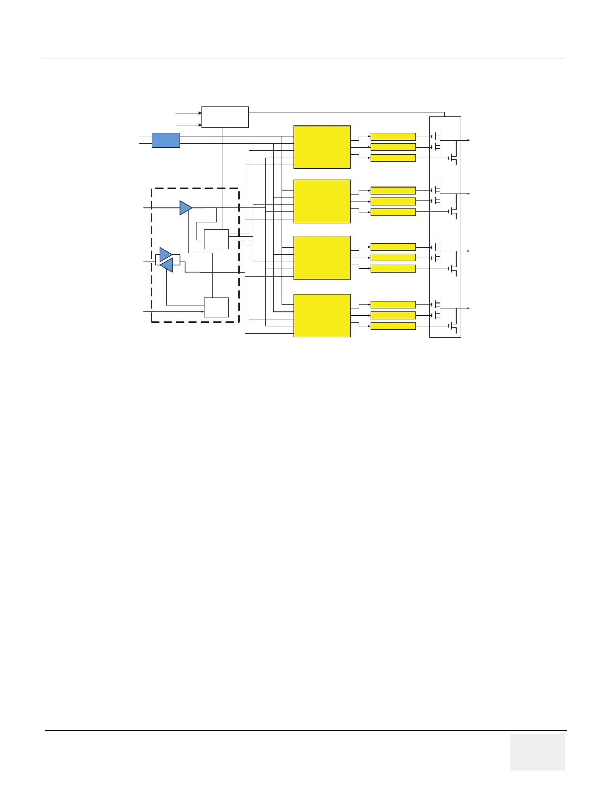
5-4-4 ATD
5-4-4-1 Overview
The ATD ASSY (Advanced Transmit Driver) generate bipolar transmit pulse for probe. This ASSY has
64 channels transmit signal drivers, Transmit Pulse Generator ASIC, control FPGA and so on. Transmit
pulse are generated by TPG2 ASIC. Each TPG2 ASIC makes 16 channels signals, so total 4 ASIC are
used in ATD assy. All of control informations for pulse generation, pulse width, time delay of each
channel are come from FEC in real time via backplane. The control FPGA, TXIC FPGA provide interfcae
between FEC and TPG2 ASICs and control operation condition of ATD assy
Main items are
* TXIC FPGA : Interface and controller FPGA. This FPGA provide the interface with FEC
assy that master of scan control.
* TPG2 ASIC: A TPG2 ASIC can generate 16 channels logic level transmit pulse signal.
This ASIC use 2 phase 40MHz clocks for transmit delay control and pulse generation.
40Mhz operation clocks are come from FEC assy via backplane.
* Transmit Pulse Driver : TPG2 ASIC generated logic level signal for transmit pulse. So this
signal need to be expanded to high voltage signal. Driver circuit make logic level signal to
high voltage level signal.
* THV Switch : LOGIQ5 system use dual transmit high voltage for transmit driver because
B mode and CFM mode use differnet voltage level of transmit pulse. So in duplex of trplex
mode, B/CFM or B/DOP, Low THV and High THV are switched in ATD assy in real time
Figure 5-8 ATD Block Diagram
FPGA
TPG2
+ T xP [15:0]
CLMP[15:0]
CLKQ1
CLKQ2
D A TA [ 15:0]
FET Driver x 16 ch
Tx Pulse[63:48]
ADDR
CS
Tx Pulse[47:32]
Tx Pulse[
31:16]
Tx Pulse[15:00]
ECL to TTL
ECL CLK 40M Q1
ECL CLK 40
M Q2
Board Select
JUSC Data
JUSC Add
ress
-TxP[15:0]
FET Driver x 16 ch
FET Driver x 16 ch
TPG2
+ T xP [15:0]
CLMP[15:0]
CLKQ1
CLKQ2
D A TA [ 15:0]
FET Driver x 16 ch
ADDR
CS
-TxP[15:0]
FET Driver x 16 ch
FET Driver x 16 ch
TPG2
+ T xP [15:0]
CLMP[15:0]
CLKQ1
CLKQ2
D A TA [ 15:0]
FET Driver x 16 ch
ADDR
CS
-TxP[15:0]
FET Driver x 16 ch
FET Driver x 16 ch
TPG2
+ T xP [15:0]
CLMP[15:0]
CLKQ1
CLKQ2
D A TA [ 15:0]
FET Driver x 16 ch
ADDR
CS
-TxP[15:0]
FET Driver x 16 ch
FET Driver x 16 ch
Buffer
Controller
Address
Controller
HV Switch
Circu
it
THV High
THV Low
 Loading...