Theory of Operation
Publication 21555, Rev. E, September 2002 3-9
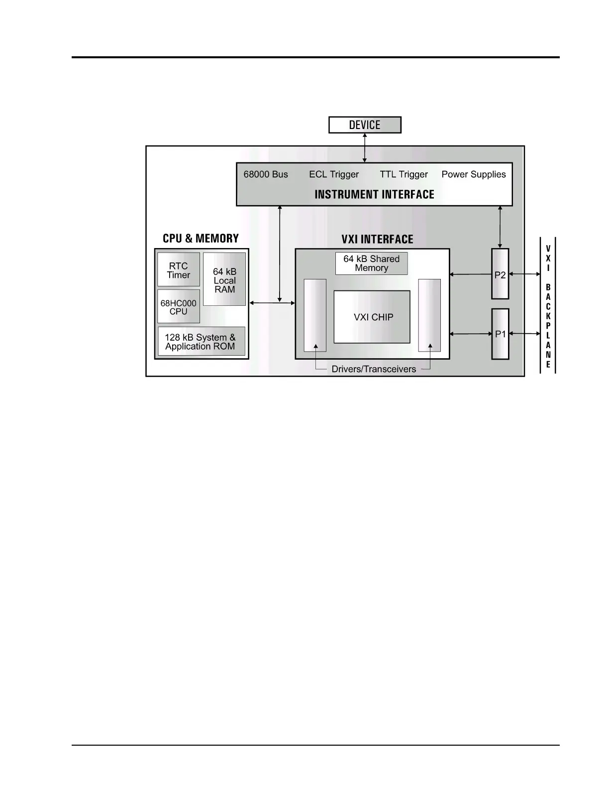
3.6 VXI Processor PC Board (A3)
The following circuit description is given for information only. The VXI Processor and Memory PC
boards are OEM assemblies. If these boards are not functioning properly, the problem will usually be
indicated by the instrument not responding to an Identification query (*IDN? - See Section 2.5.30). See
Section 5.3 for replacement instructions.
The VXI Processor PC Board circuit functions are divided into three main sections:
• VXI Interface
• CPU and Memory
• LEDs and Drivers
3.6.1 VXI Interface
The VXI interface contains 64 kB of Shared Memory, a VXI interface gate array, and the drivers and
transceivers to enable the VME and CPU to access the Shared Bus.
3.6.1.1 VXI Gate Array
U28 is a 120-pin gate array, packaged in a 13x13-pin grid array. The gate array generates the necessary
signals that control the flow of data from the processor section through the shared bus, and to the VXI
bus, and vice versa.
The gate array also controls the LEDs that indicate whether the VXI is accessing the VXI A16 or the
A24/A32 registers, and the FAIL LED, which indicates whether the VXI A16 registers have been
initialized.
Figure 3-5: VXI Processor (A3) Block Diagram