Evaluation Board Manual
Preliminary PPC750FX Evaluation Board
750FXebm_ch10.fm
June 10, 2003
Connectors
Page 67 of 115
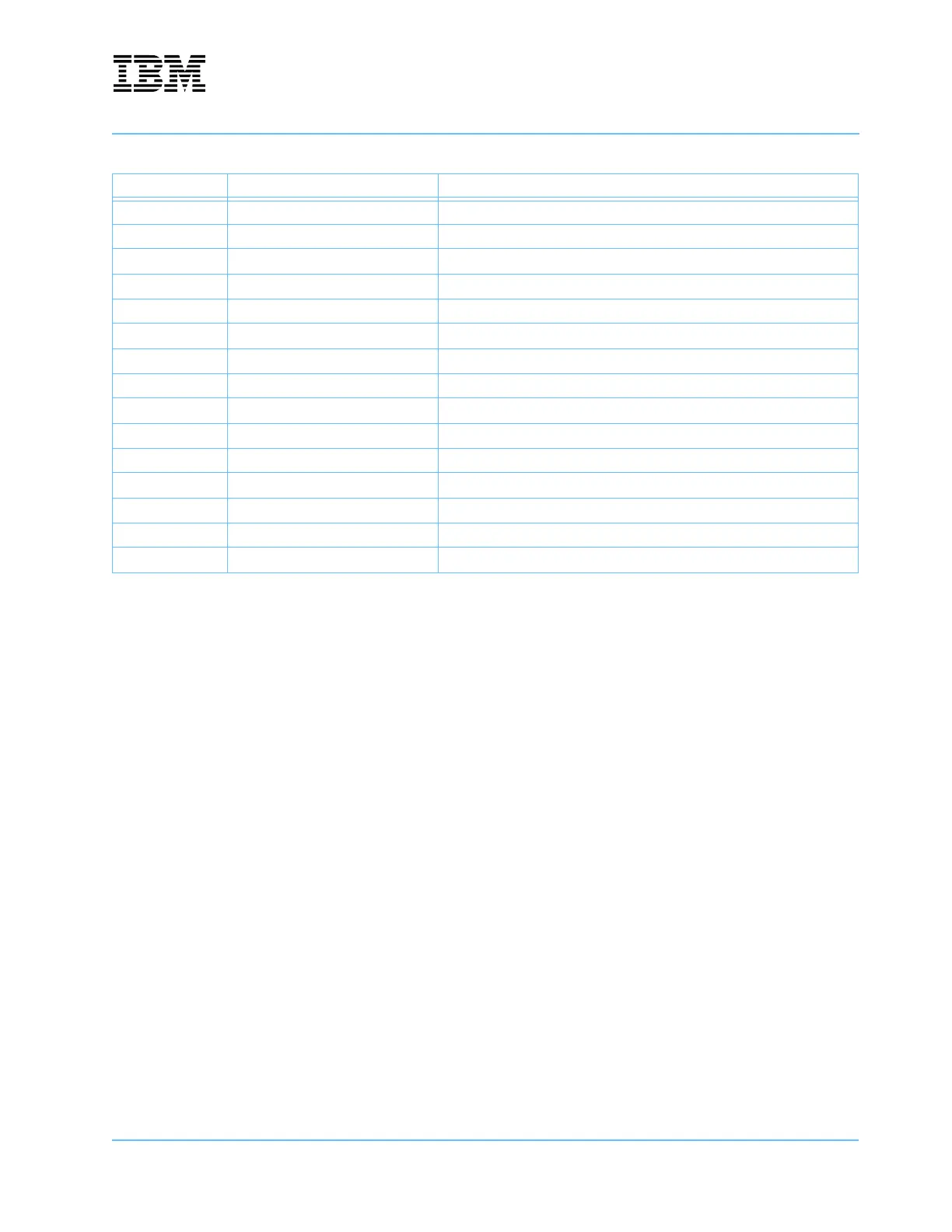
24 cntl_pod1 – D7 CPU0_HRESET_2.5_N
25 cntl_pod0 – D6 NVRAM_CS_N
26 cntl_pod1 – D6 CPU0_SRESET_2.5_N
27 cntl_pod0 – D5 BIG_FLASH_CS_N
28 cntl_pod1 – D5 unused
29 cntl_pod0 – D4 SMALL_FLASH_HI_CS_N
30 cntl_pod1 – D4 TESTPIN_D
31 cntl_pod0 – D3 SRAM_HI_CS_N
32 cntl_pod1 – D3 TESTPIN_B
33 cntl_pod0 – D2 READ_N
34 cntl_pod1 – D2 unused
35 cntl_pod0 – D1 WRITE_N
36 cntl_pod1 – D1 FPGA_CS_N
37 cntl_pod0 – D0 UART_CS_N
38 cntl_pod1 – D0 TESTPIN_C
Table 10-11. Memory Control Signals—J15 (Continued)
Pin Analyzer Signal Name