Evaluation Board Manual
Preliminary PPC750FX Evaluation Board
750FXebm_ch11.fm
June 10, 2003
CPLD Programming
Page 73 of 115
11. CPLD Programming
This chapter contains logic of the CPLD (formerly FPGA) module and timing values for the signals associated
with the CPLD.
11.1 Programming—Registers and Control Functions
General software functions such as address decoding and board status registers are provided by the CPLD
at U29. The following figures provide a combined graphical and textual representation of the functional
programming within the CPLD.
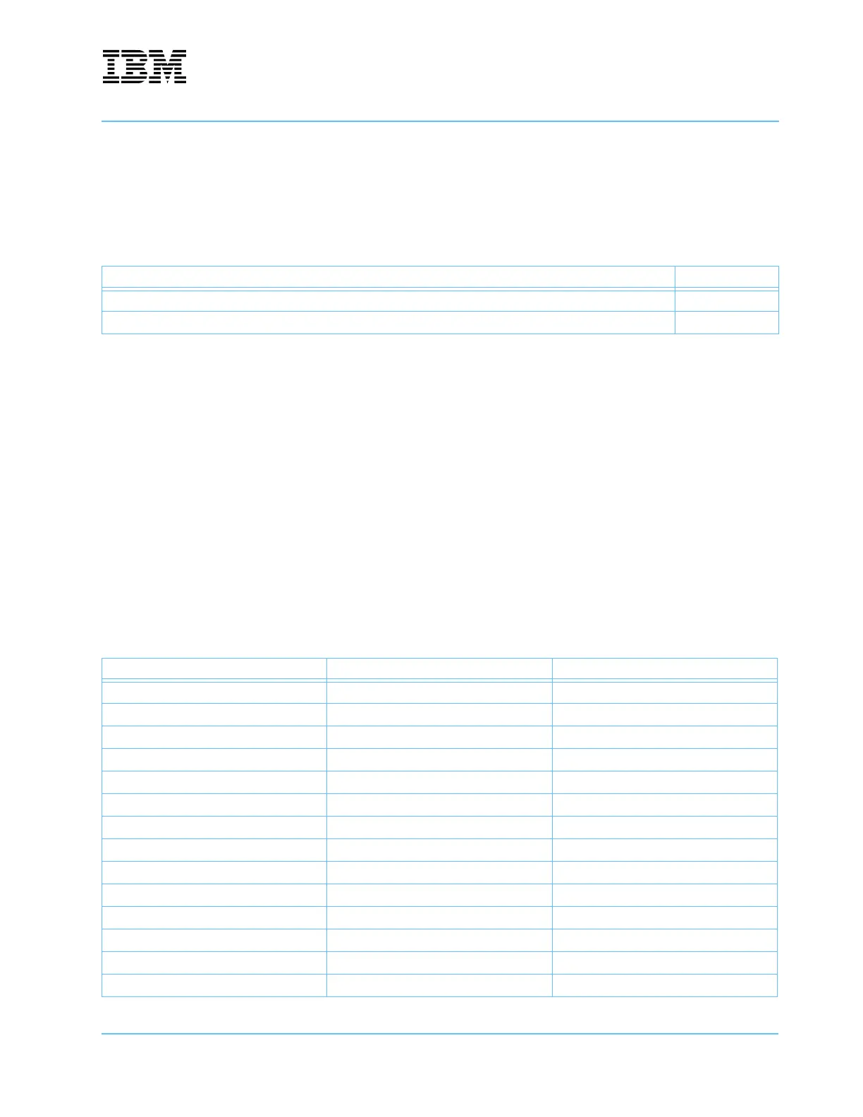
11.1.1 I/O Pin List
Table 11-2 lists all of the signals entering and exiting the CPLD module. The module pin number and I/O
function are shown.
Note: Pins that are labeled as
∼NAME∼ are special purpose pins defined by the CPLD to program functions
or set reference voltages.
Table 11-1. Section Contents
Description Page
Programming—Registers and Control Functions 73
Timing—Registers and Control Functions 94
Table 11-2. CPLD I/O Pin List
Name Pin Function
cpu0_chkstop_n 1 Input
ale 2 Input
VCCIO1 3 Power
~TDI~ 4 Input
rw_trst 5 Input
sram_hi_cs_n 6 Output
small_flash_hi_cs_n 7 Output
badr[1] 8 Input
led0 9 Output
led2 10 Output
GND 11 Gnd
~VREFA~ 12 Input
fpga_cs_n 13 Output
pci_reset_n 14 Bidir