Key RVP Features and Block Diagrams
14 Intel Confidential User Guide
3 Key RVP Features and Block
Diagrams
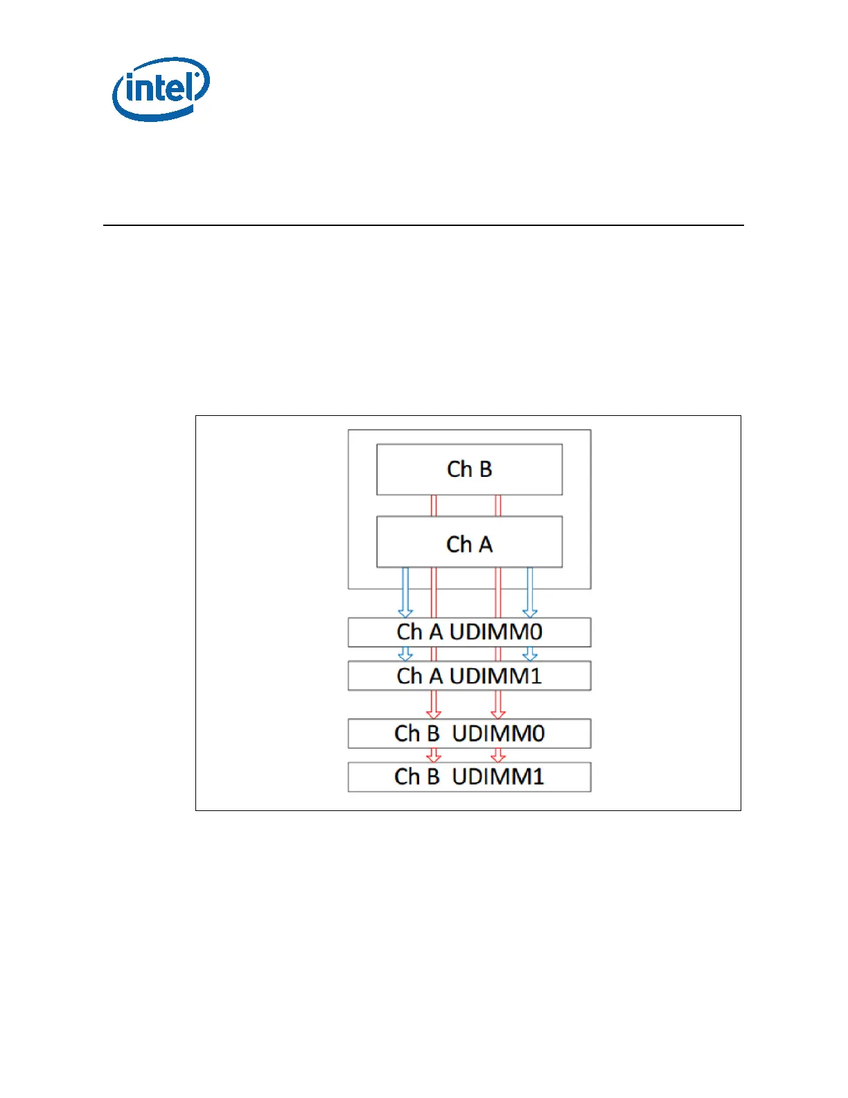
3.1 DDR4 Memory Topology
• UDIMM/SODIMM DRR4
− 2DPC:2666
− The CFL-S RVP follows interleaved memory configuration for 2DPC DDR4
routed in T-topology.
− ECC is supported in 4 layer topology based on SI topology
Figure 2. DDR4 Memory Topology Diagram (Shows Only UDIMM)
3.2 Clock
The CNP-H chipset is the primary clock generator for all sub-system and CPU clocks
on the CFL-S RVP. All the sub-system clocks and external clock outputs are derived
through internal PLLs. A high level block diagram of the chipset clock interface is given
below




 To Next Page