2KA
2-3-41
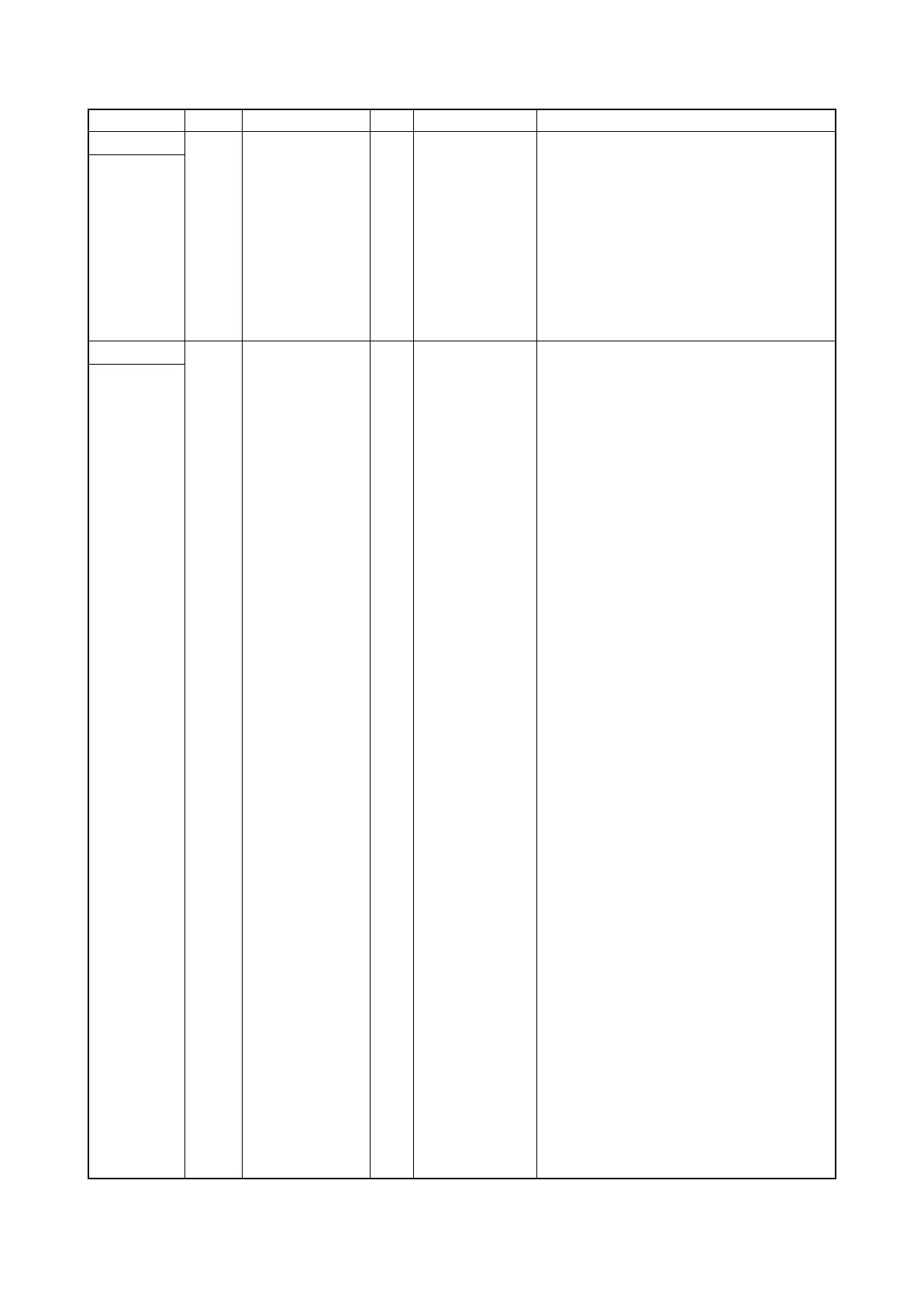
Connector Pin No. Signal I/O Voltage Description
YC1 1 +3.3V I 3.3 V DC 3.3 V DC power to OPPWB
Connected to
the main
PWB
2 GND - - Ground
3 FPRST I 0/3.3 V DC OPPWB reset signal
4 FPTXD I 0/3.3 V DC (pulse) OPPWB serial communication data signal
5 FPD_SEL I 0/3.3 V DC OPPWB select signal
6 FPCTS O 0/3.3 V DC OPPWB control signal
7 FPRXD O 0/3.3 V DC (pulse) OPPWB serial communication data signal
8 GND - - Ground
9 +5V1V I 5 V DC 5 V DC power to OPPWB
YC2 1 GND - - Ground
Connected to
the LCD
2V0 -- Ground
3V4 -- Ground
4V3 -- Ground
5V2 -- Ground
6V1 -- Ground
7 C2N I 0/3.3 V DC LCD control signal
8 C2P I 0/3.3 V DC LCD control signal
9 C1P I 0/3.3 V DC LCD control signal
10 C1N I 0/3.3 V DC LCD control signal
11 C3P I 0/3.3 V DC LCD control signal
12 VOUT - - Ground
13 VSS - - Ground
14 VDD
O 3.3 V DC 3.3 V DC power to LCD
15 SI O 0/3.3 V DC (pulse) LCD serial communication data signal
16 LCLK O 0/3.3 V DC (pulse) LCD clock signal
17 A0 O 0/3.3 V DC LCD control signal
18 RESN O 0/3.3 V DC LCD reset signal
19 CS1N O 0/3.3 V DC LCD control signal
20 GMD - - Ground
 Loading...