6
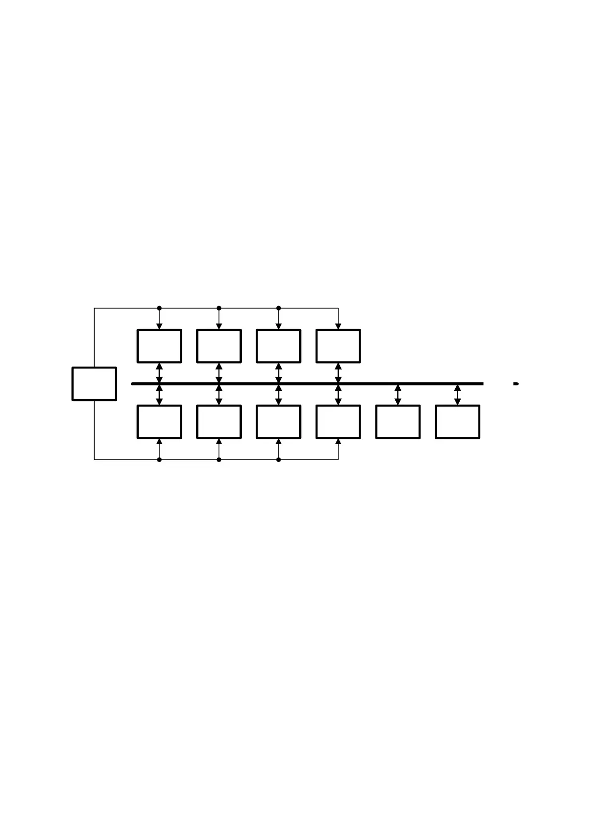
Using the MAC register simplifies programming for MIMO. As an example, the
addresses of registers controlling TBBA and TBBB are the same, but the individual A or B
channels are identified using the MAC[1:0] register.
Let us consider the write operation to the G_TIA_RFE_A[1:0] register. This register
controls the RFE module within MIMO channel A. To write to the G_TIA_RFE_A[1:0]
register, we have to set MAC[1:0] to the "01". If we set MAC[1:0] to the "11" then the same
value will be written to the registers G_TIA_RFE_A[1:0] and G_TIA_RFE_B[1:0] at the
same time (i.e. only one write operation is required, hence time saved). Similarly, if we want
to write to the G_TIA_RFE_B[1:0] register only, we have to set MAC[1:0] to "10".
The special case is frequency synthesizers SXR and SXT. Register addresses are the
same for SXR and SXT. To control SXT we have to set MAC[1:0] to the "10" and MAC[1:0]
to the "01" for SXR.
Modules from the Top and Other logical blocks (see Table 1) are not controlled by the
MAC[1:0] register.
TRXA
Block
TXA
Block
RXA
Block
TRXB
Block
TXB
Block
RXB
Block
Top
Block
Other
Block
SPI Bus
MAC[0]
MAC[1]
MIMO channel A
control enable
MIMO channel B
control enable
SXR
SXT
Figure 4 Access logic of configuration modules
The memory mapping is shown in Table 1. There are five basic logical blocks. These
are:
a) Other, controlling the microcontroller and LimeLight
TM
interface;
b) Top, controlling the top level bias, clock synthesizers, buffers, LDOs and BIST;
c) TRX, controlling the Transmit and Receive RF functions;
d) TX, controlling the transmit digital functions;
e) RX, controlling the receive digital functions.