HELIOS LED Processing Platform - USER GUIDE
22
Creating Maps
The HELIOS Processor uses a map to determine which segments of the incoming raster to consider as an ‘active pixel
region’. Areas of the incoming raster that are not associated with display xtures, are never transmitted to the system. If
only two xtures are mapped, only two xtures worth of panel data is transmitted.
If tiles have been discovered they will be placed on the map. By default, when panels are discovered, they are all stacked
in the top left (0,0) position. HELIOS does not support ofine mapping. Only automatically discovered tiles can be
mapped.
The thin light gray line on the outside of the tile region marks the boundaries of an 8192 x 4320 pixel space. It can be
used as a guideline for placement, but maps do not need to be constrained to it. On a layer below the colored panel
icons is a preview of the selected input (or a grey rectangle if the input is unavailable) that represents the incoming signal’s
raster area. It will only be visible if the input signal raster is set larger (using the Input pane) than the space occupied by
the tiles. In the example below it is slightly oversized to the panels.
The mapping tools at the bottom of the page are used to move the panels into the positions that they occupy in the
physical system. Select a group of panels, dene the columns and rows that they should be arranged in, then select the
cable order. When the cable order icon button is pressed, the selected panels will be re-ordered. HELIOS can undo and
redo maps incase something did not turn out as desired. Panel locations can also be adjusted manually by drag and drop
or by typing the desired X and Y coordinates.
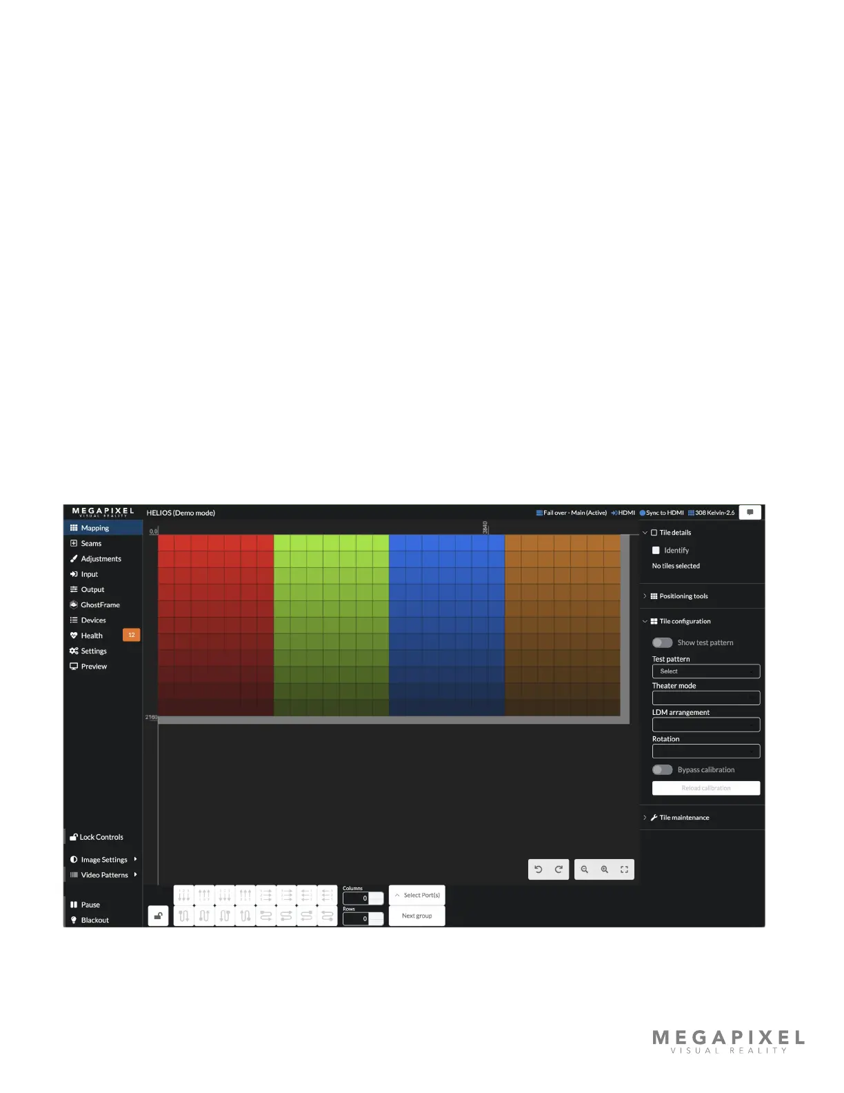
Display panels are tinted according to the network switch that the panels are connected to (Red = 1, Green =2, Blue = 3
etc.). In the example below the system has been cabled in columns with seven columns per port. There are four network
switches in the system example below.
Figure 25: Mapping pane.