Chapter 3
MIPS® Malta™ User’s Manual, Revision 01.07 13
Copyright © 2000-2007 MIPS Technologies Inc. All rights reserved.
Memory Map
This chapter describes the Malta Board’s memory map and its control/status registers as seen by the CPU. The mem-
ory map showing the starting addresses of the major devices on the board is shown in Table 3.1.
Note: Address 1FC0.0010 in Flash memory is “special”—a read from this address reads the contents of the Revision
register, allowing software to identify the hardware environment and configure itself accordingly. The next address,
1E00.0010, decodes to an address in Flash memory.
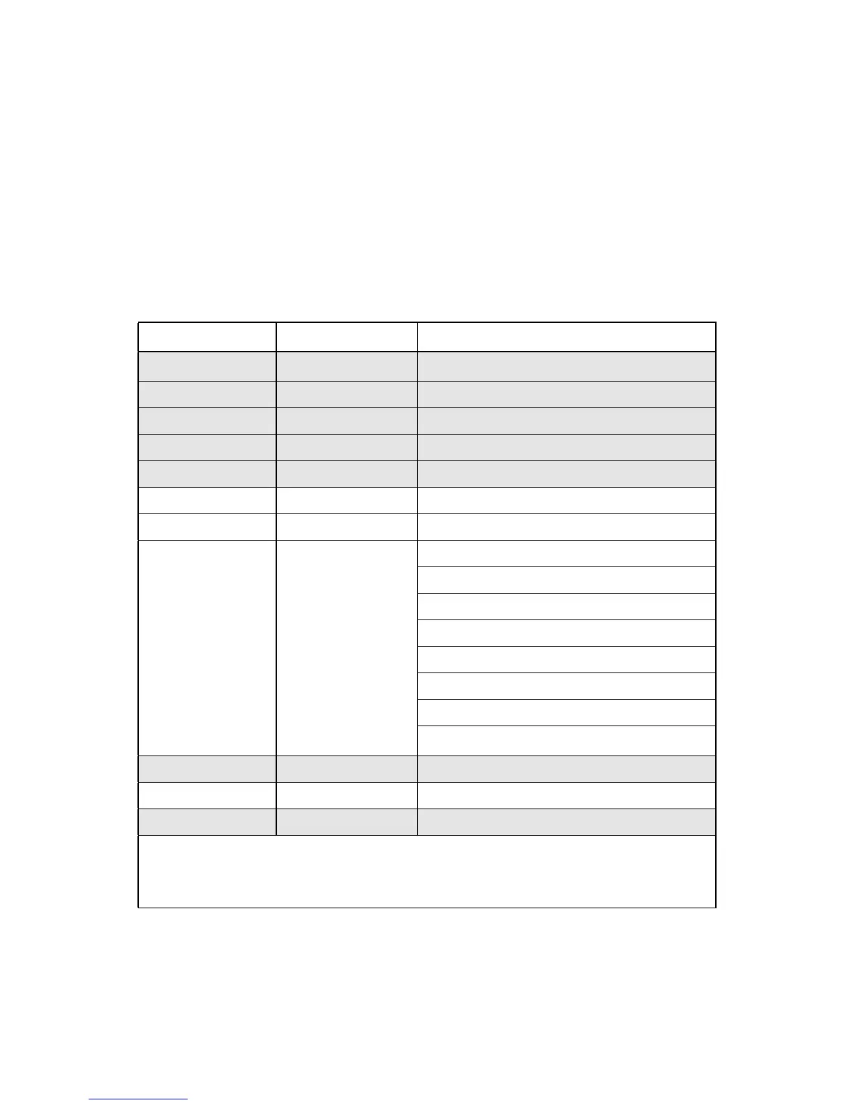
Table 3.1 Malta Physical Memory Map
Base Address Size Function
0000.0000
(*)
128Mbytes Typically SDRAM (on Core Board)
0800.0000 256 Mbytes Typically PCI
1800.0000 62 Mbytes Typically PCI
1BE0.0000 2 Mbyte Typically System controller’s internal registers
1C00.0000 32 Mbytes Typically not used
1E00.0000 4 Mbytes Monitor Flash
1E40.0000 12 Mbytes Reserved
1F00.0000 12 Mbytes Switches
LEDs
ASCII display
Soft reset
FPGA revision number
CBUS UART (tty2)
General purpose I/O
I
2
C controller
1F10.0000 11 Mbytes Typically System Controller specific.
1FC0.0000 4Mbyte Maps to Monitor Flash
1FD0.0000 3 Mbytes Typically System Controller specific.
The shaded area of the table indicate memory areas whose mapping depends on the implementation of the
Core Board and on software.
The memory area 000F.0000-000F.FFFF (PC BIOS area) is only accessible from the CPU and not from the
PCI bus (the South Bridge decodes this memory area).