3.5 Displays
MIPS® Malta™ User’s Manual, Revision 01.07 17
Copyright © 2000-2007 MIPS Technologies Inc. All rights reserved.
3.5 Displays
There are 2 display devices on the board: an 8-LED array (D28 is a 10-LED, but only 8 are used), and an 8-character
ASCII display (U42). These are controlled using the registers shown in Table 3.9 through Table 3.12.
3 S54 DIP switch S5-4.
YAMON use this switch.
“1” will set YAMON in factory default mode
(communication on tty0, etc.).
n/a
2 S53 DIP switch S5-3 n/a
1 BIGEND “1” indicates big endian mode, as controlled by
switch S5-2.
n/a
0 Reserved Reserved 0
Name: JMPRS
Address: 0x1F00.0210
Access: RO
Reset Value: n/a
Table 3.8 JMPRS Register
Bits Field Name Function Initial Value
31:5 Reserved Reserved 0
4:2 PCICLK PCI clock frequency 10-37.5MHZ
See Table 4.2
Bit 4 is Pins 5-6
Bit 3 is Pins 3-4
Bit 2 is Pins 1-2
“1” = jumper fitted
n/a
1 EELOCK
State of JP2: Not fitted ~ “1” =
I
2
C EEPROM
write protected.
n/a
0 Reserved Reserved 0
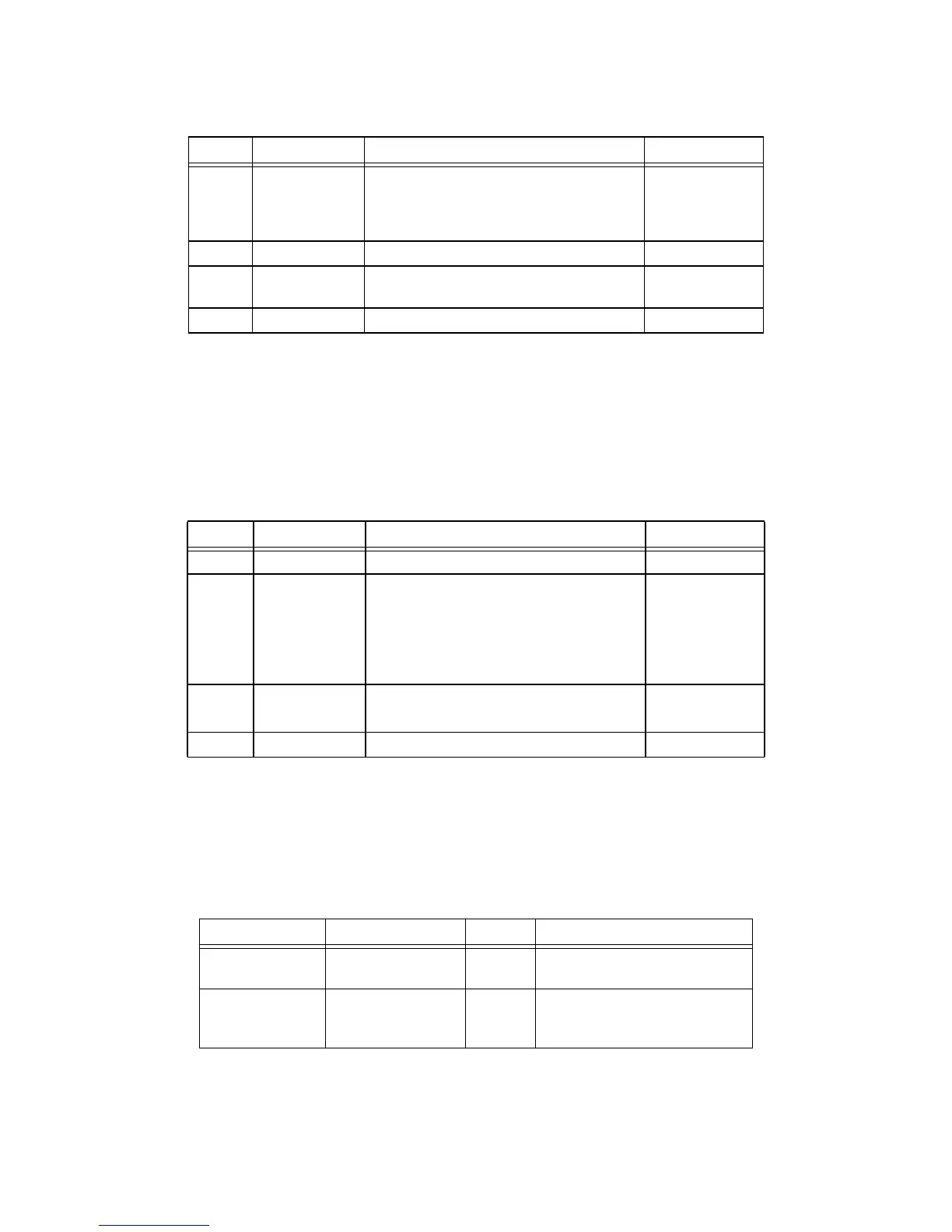
Table 3.9 Display Registers. BASE = 0x1F00.0400
Register Name Offset Address Access Function
LEDBAR 0x0000.0008 R/W 8 bits each corresponding to 1 LED.
1 = ON
ASCIIWORD 0x0000.0010 WO Writing a 32-bit word to this register
will cause it to be displayed in hex
on the ASCII character display.
Table 3.7 STATUS Register (Continued)
Bits Field Name Function Initial Value