Core Card Design
50 MIPS® Malta™ User’s Manual, Revision 01.07
Copyright © 2000-2007 MIPS Technologies Inc. All rights reserved.
7.1.7 Endian
The endian control signal, BIGEND, is driven by the motherboard according to setting of S5-2.
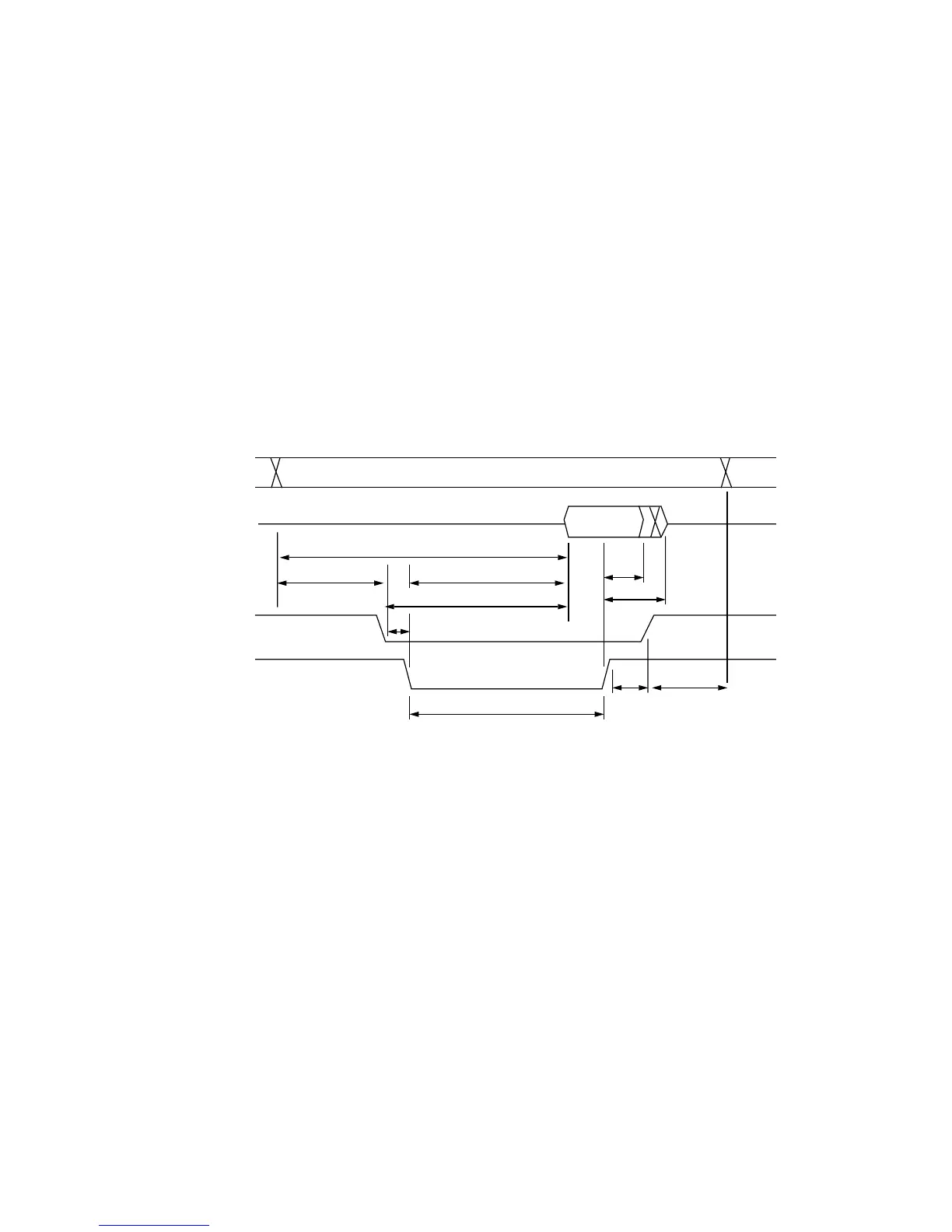
7.1.8 CBUS
The CBUS is designed to interface to simple devices on the motherboard which must be accessed by the CPU before
the PCI is up and running, or to devices with a low latency (for example, the interrupt controller and Flash memory).
CBUS signals are described in Table 7.2.
All core cards decode CPU addresses from 0x1C00.0000 to 0x1FFF.FFFF. These addresses are translated to
addresses 0x0000.0000 to 0x03FF.FFFF on the CBUS.
All CBUS signals must use 3.3 volt signalling levels. Read and write cycles are schown in Figure 7.1and Figure 7.2.
AC timing parameters are shown in Table 7.1.
Figure 7.1 CBUS Read Cycle
CD[31:0]
CCSN
CRDN
ADDR
T2
T0
T1
T4
RD DATA
T7
T5
T3
CA[25:2]
T6
T12
T13