7.2 Signals
MIPS® Malta™ User’s Manual, Revision 01.07 53
Copyright © 2000-2007 MIPS Technologies Inc. All rights reserved.
7.2.1 J3 Connector
The pin list for the J3 connector is shown in Table 7.3.
D5V Input - - 5 Volt power
D3V3 Input - - 3.3 Volt power
CPWR_OK Input - - Indicates that power on both 3V3 and 5V rails
is up.
CORE_OK Output - up Indicates that Core is ready to come out of
reset.
RSTN Input - - Global reset signal.
PCI_AD[31:0] I/O - - PCI bus
PCI_DEVSEL
N
I/O - - PCI bus
PCI_CBEN[3:0
]
I/O - - PCI bus
PCI_REQN Output - - PCI bus
PCI_GNTN Input - - PCI bus
PCI_SERRN I/O - - PCI bus
PCI_FRAMEN I/O - - PCI bus
PCI_IRDYN I/O - - PCI bus
PCI_IDSEL I/O - - PCI bus
PCI_PAR I/O - - PCI bus
PCI_STOPN I/O - - PCI bus
PCI_CLK Input - - PCI bus
PCI_TRDYN I/O - - PCI bus
PCI_LOCKN I/O - - PCI bus
PCI_PERRN I/O - - PCI bus
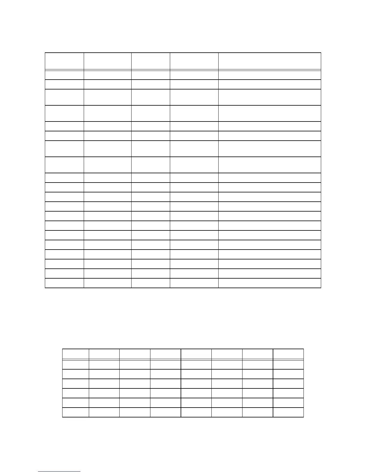
Table 7.3 J3 Pin List
Number Name Number Name Number Name Number Name
1 CPWR_OK 51 GND 101 D3V3 151 SCK
2 JTGCPU 52 D5V 102 GND 152 CGPI4
3 CINTHIN 53 GND 103 GND 153 SDA
4 CORE_OK 54 CINTLON 104 GND 154 CGPO7
5 CGPI7 55 GND 105 D3V3 155 CGPO6
6 CD31 56 D5V 106 GND 156 CGPO5
Table 7.2 Core Card Interface Signals (Continued)
Signal
Direction (from
Core Card)
Pull (on Core
Card)
Pull (on
Motherboard) Description