Memory Map
22 MIPS® Malta™ User’s Manual, Revision 01.07
Copyright © 2000-2007 MIPS Technologies Inc. All rights reserved.
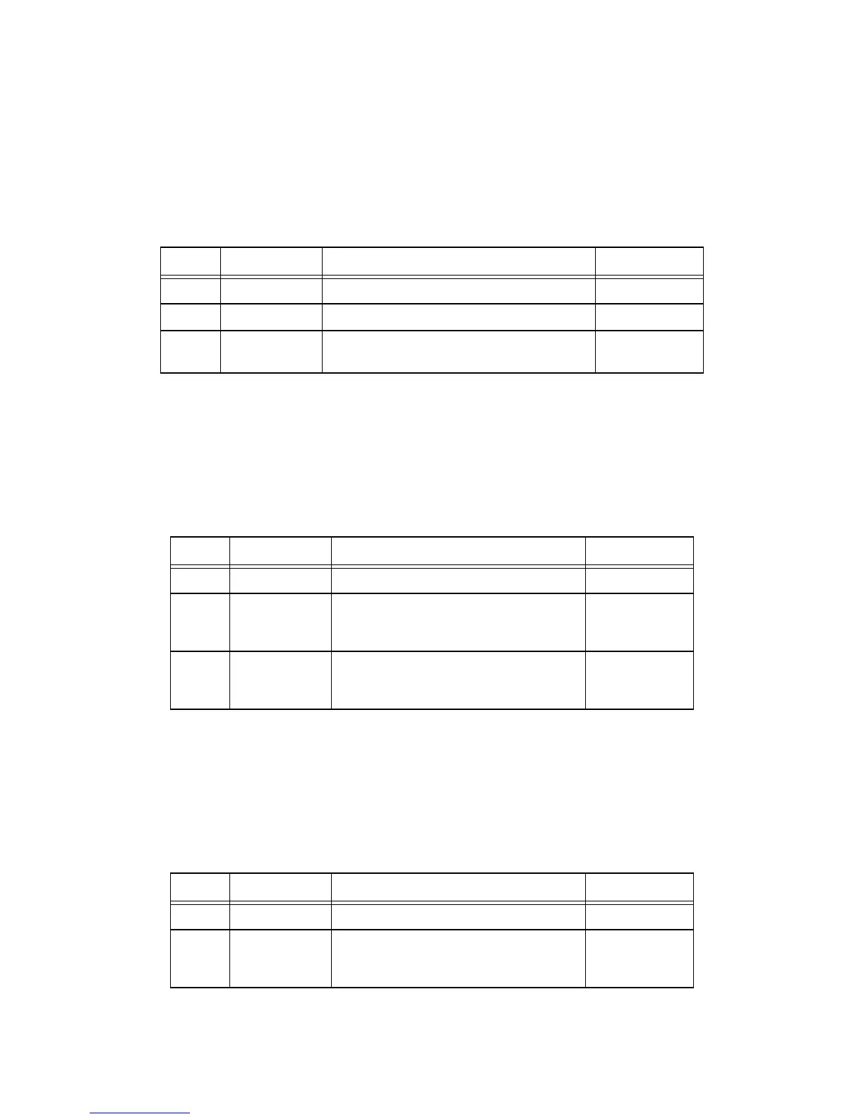
Name: I2CINP
Address: 0x1F00.0B00
Access: RO
Reset Value: n/a
Table 3.18 I2CINP Register
Bits Field Name Function Initial Value
31:2 Reserved Reserved n/a
1 I2CSCL Reading gives the actual value of the I2C SCL pin. 1
0 I2CSDA Reading gives the actual value of the I2C SDA
pin.
1
Name: I2COE
Address: 0x1F00.0B08
Access: R/W
Reset Value: n/a
Table 3.19 I2COE Register
Bits Field Name Function Initial Value
31:2 Reserved Reserved n/a
1 I2CSCL “1” means that the I2CSCL bit of the I2COUT
register will be driven to the I2C SCL pin.
“0” means that the I2C SCL pin is tri-stated.
0
0 I2CSDA “1” means that the I2CSDA bit of the I2COUT
register will be driven to the I2C SDA pin.
“0” means that the I2C SDA pin is tri-stated.
0
Name: I2COUT
Address: 0x1F00.0B10
Access: R/W
Reset Value: n/a
Table 3.20 I2COUT Register
Bits Field Name Function Initial Value
31:2 Reserved Reserved n/a
1 I2CSCL The value of this bit will be driven to the I2C
SCL pin when the I2CSCL bit of the I2COE
register is “1”.
1