7.1 Required Interfaces
MIPS® Malta™ User’s Manual, Revision 01.07 51
Copyright © 2000-2007 MIPS Technologies Inc. All rights reserved.
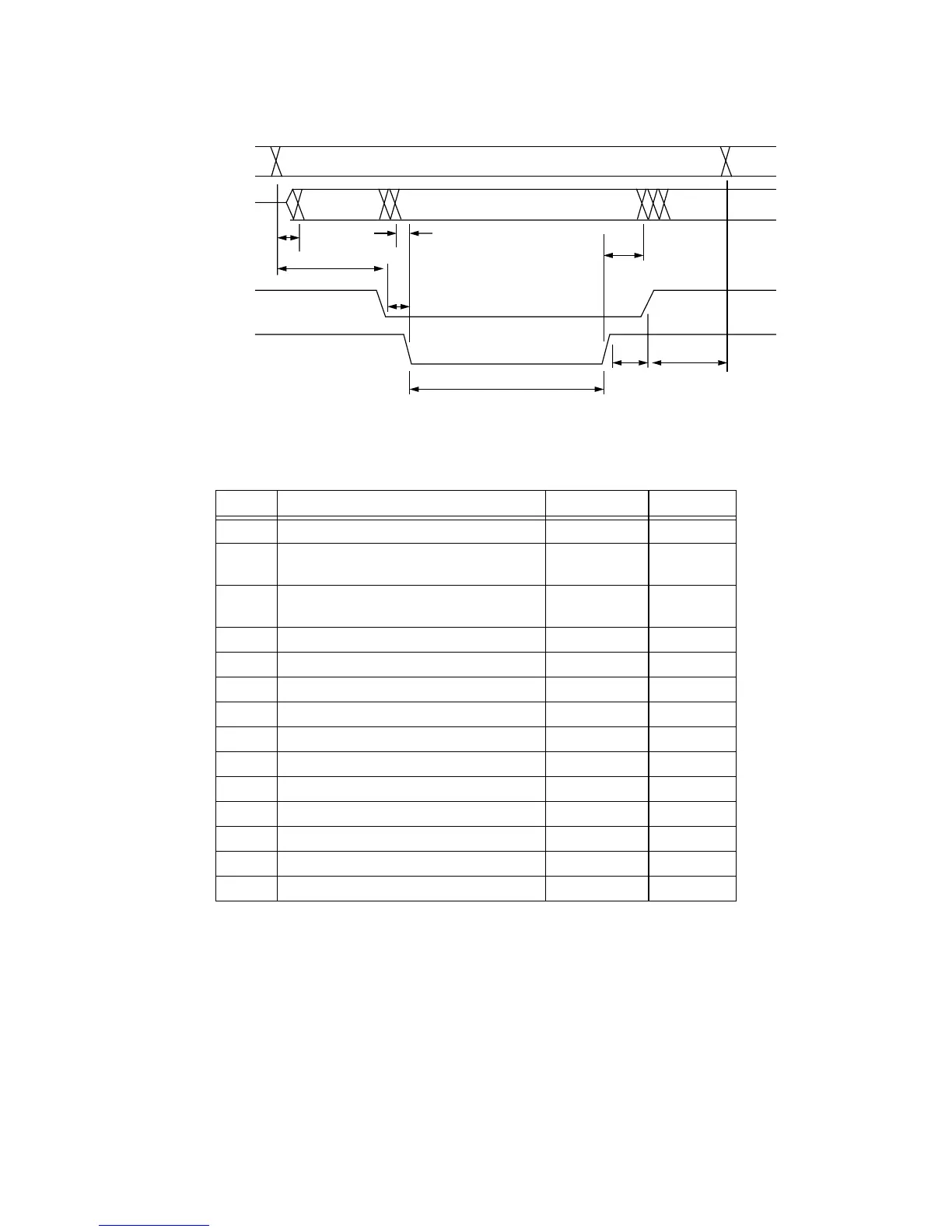
Figure 7.2 CBUS Write Cycle
7.1.9 EJTAG
The EJTAG signals from the “basic” EJTAG connector are taken to the interface from the front panel connector.
7.1.10 Misc.
Various debug, reserved, and presence-detect functions, as described in the following subsections.
Table 7.1 CBUS AC Timing Parameters
Ref Description Tmin(ns) Tmax(ns)
T0 Address valid to CCSN active 5 -
T1
CCSN valid to strobe (CRWN or CRDN)
valid
10 -
T2
strobe (CRWN or CRDN) inactive to
CCSN inactive
10 -
T3 Address hold from CCSN inactive 20 -
T4 CRDN width 120 -
T5 CRDN active to read data valid - 120
T6 CRDN inactive to data bus tristated - 20
T7 Read data hold time after CRDN inactive 0 -
T8 Address valid to data bus driven 0 -
T9 Write data setup to CRWN active 0 -
T10 Write data hold time after CWRN inactive 10 -
T11 CWRN pulse width 75 -
T12 Address valid to read data valid - 150
T13 CCSN active to read data valid - 150
CD[31:0]
CCSN
CWRN
ADDR
T2
T0
T1
T11
T8
T10
T3
CA[25:2]
T9
WR DATA