Memory Map
14 MIPS® Malta™ User’s Manual, Revision 01.07
Copyright © 2000-2007 MIPS Technologies Inc. All rights reserved.
RAM is typically mapped at the bottom of memory, so that exception vectors are located in fast memory.
Malta does not specify a mapping for addresses above 0x2000.0000. These addresses are accessed via kuseg, using
mapping defined by TLB entries.
The I
2
C bus (called the SMB bus in the Intel documentation) is controlled by the CBUS FPGA (it can also be con-
trolled by the controller in the South Bridge). The I
2
C bus address map is shown in Table 3.2.
Note that all addresses shown are physical addresses. You should use the macros in the header files to access all reg-
isters and fields [3].
All registers are addressed as 32-bit words, on 64-bit word boundaries. This convention allows software to access all
registers using the same word address in both big- and little-endian modes. Those registers that contain a single value
are not described in bit-field detail; these values occupy the least-significant bit of the register.
3.1 Revision Information
The Revision register contains information about the revision of the Malta and Core Boards.
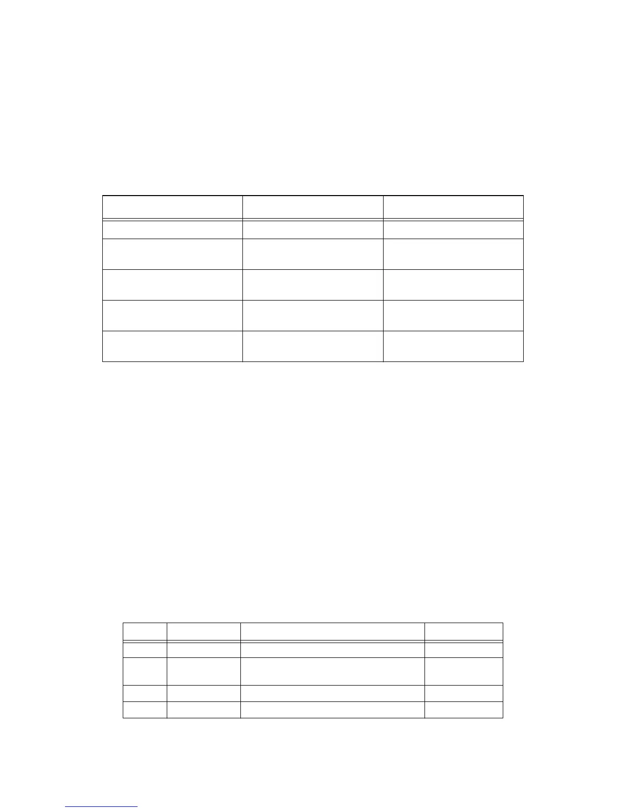
Table 3.2 I
2
C Slave Address Map
I
2
C Slave Address Size Function
0x50 256 bytes Core Board, PC-100 SDRAM
0x51 256 bytes Core Board, optional PC-100
SDRAM
0x52 256 bytes Core Board, optional PC-100
SDRAM
0x53 256 bytes Core Board, optional PC-100
SDRAM
0x54-0x57 1024 bytes Malta EEPROM - read-only
Contains serial number
Name: REVISION
Address: 0x1FC0.0010
Access: RO
Reset Value: n/a
Table 3.3 REVISION Register
Bits Field Name Function Initial Value
31:24 Reserved Reserved 0
23:16 FPGRV 8-bit binary number gives revision of CBUS
FPGA.
n/a
15:10 CORID 6-bit Core Board ID n/a
9:8 CORRV 2-bit Core Board revision n/a