Board Layout
26 MIPS® Malta™ User’s Manual, Revision 01.07
Copyright © 2000-2007 MIPS Technologies Inc. All rights reserved.
The board has an ATX (305 mm x 244mm) form factor and is in accordance with the ATX specification [12] with
regards to board size, mounting hole placement, connector placement, and height constraints.
The connector layout on the rear panel (namely, the shield design as described in Design Guide for Intel ATX Moth-
erboard I/O Implementations Version 1.1 [13] is a subset of Intel Core design #1. This enables the Malta Board to be
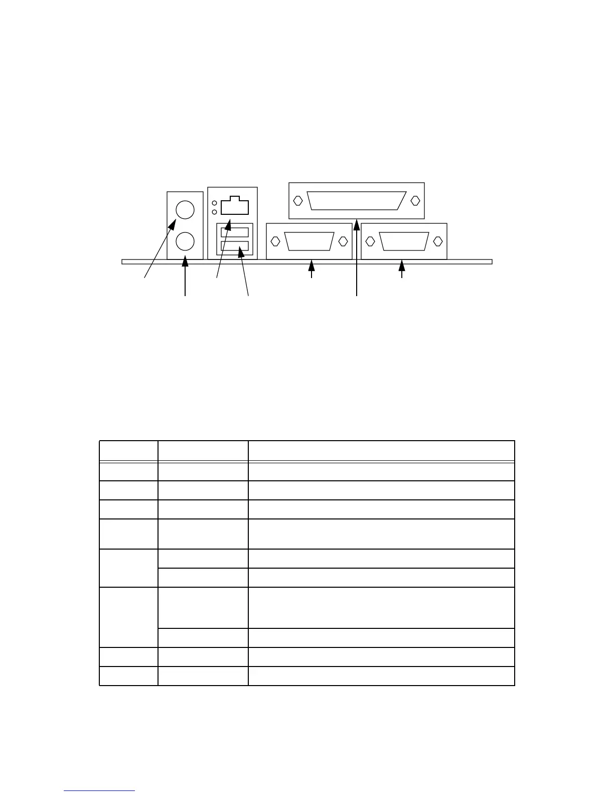
installed in an ordinary ATX chassis. Figure 4.2 shows the rear panel connector layout.
Figure 4.2 Rear Panel Connector Layout
4.1 Connectors & Jumpers
All jumpers are standard 0.1” pitch. A dot by a pin indicates pin 1. On all jumpers, pins are numbered crosswise, that
is, the end pins are 1 & 2 (this is not always the case on other connectors).
Table 4.1 Interface Connectors
Ref Type Description
J1 10 pin 0.1” header Download connector for CBUS FPGA EEPROM.
J2 10 pin 0.1” header Download connector for Arbiter EPLD.
J3 200way header Connects the Core Board. Carries amongst other things the CBUS.
J4 200way header Connects the Core Board. Carries amongst other things the primary
PCI bus.
J5 RJ45 Ethernet.
Dual USB A Two USB host ports.
J6 25 pin DSUB IEEE1284 / Flash programming port. This can either be used as a par-
allel port for communications, and is also used to program Flash
devices during production.
Dual 9 pin DSUB tty0 (left) and tty1 (right).
J7 Dual 6 pin miniDIN Connection to a PC keyboard (lower) and mouse (upper).
J8 ATX PSU This connects the power.
Keyboard
Dual USB
Parallel Port (1284)
Serial Port (tty0) Serial Port (tty1)
Mouse
Ethernet