May 25, 2005 6881096C74-B
4-14 Troubleshooting Procedures: UHF Range 1 (380–470 MHz) Band Main Board Troubleshooting
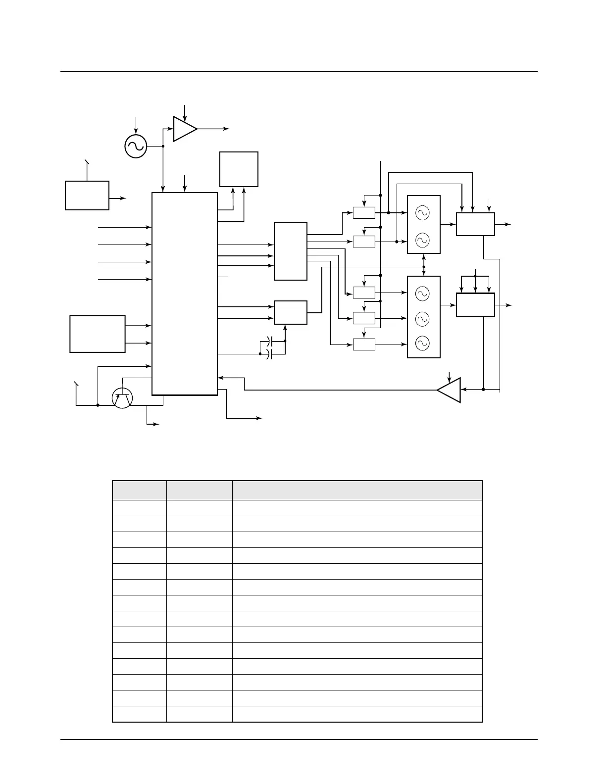
Figure 4-5. Frequency Generation Unit Block Diagram (UHF Range 1)
Table 4-9. LV Frac-N U6751 Pin Descriptions (UHF Range 1)
Pin No. Pin Name Description
1
AUX2 Auxiliary logic output
2
AUX3 Auxiliary logic output
3
AUX4 Auxiliary logic output
4
LOCK Lock detect—logic high indicates in-lock condition
5
PD_VDD 3.0-V supply (phase detector)
6
GROUND Ground (digital)
7
DATA SPI data I/O
8
CLK SPI clock
9
CEX SPI enable line—active low
10
MODIN Modulation input from controller
11
VMULT4 Multiplier clock output
12
VMULT3 Multiplier clock output
13
VRO 3.0-V supply for reference oscillator warp circuitry
14
VMULT2 Not used
Bias 1
3.0V
3.0V
3.0V
3.0V
8.2V
Lock Detect
to Controller
Prescaler Input
Q5755
RF
Feedback
8.2V
Bias 2
9.3V
SFIN
SFBASE
SFOUT
Lock
PREIN
AUX4
AUX3
Mod Out
IADAPT
IOUT
AUX2
AUX1
VMULT4
VMULT3
5.0V
16.8MHz Reference
to Controller and
Receiver Back End
VOLTAGE
MULTIPLIER
D5750 and
D5751
16.8MHz OSC
8.2V
Super Filter
Q5752
U5751
U5752
3.0V
Regulator
U5750
PHASE
DETECTOR BIAS
Q5750 RX and
Q5751 TX
CLOCK
SYN_SEL
DATA
MOD_IN
From
Controller
NC
A
X0
X1
X2
X3
X4
B
C
7.5V
8.2V
Q5706
Q5707
Q5708
Q5709
RX
INJECTION
TX
INJECTION
RX
Injection
TX
Injection
Keyed
9.1V
C5779
C5780
LOOP
FILTER
8.2V SW
8.2V SW
8.2V SW
8.2V SW
Q5825
Q5826
Q5901
Q5903
Q5905
U5753
Q5710
8.2V SW
 Loading...