6881096C74-B May 25, 2005
Theory of Operation: Transmitter 3-33
3.6.2.2 100-Watt Transmitter
The following text discusses the 100-W transmitter.
3.6.2.2.1 RF Power Amplifier (RFPA)
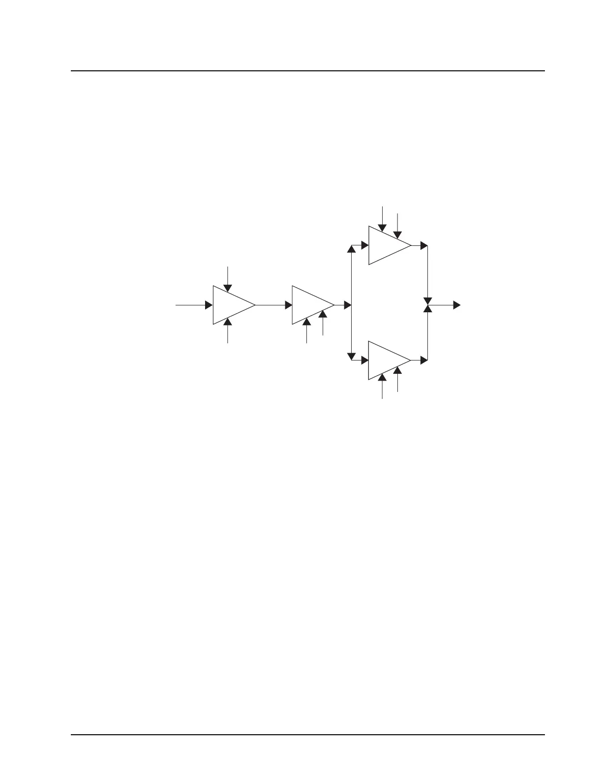
The RFPA consists of three gain stages, which are shown in Figure 3-26.
Figure 3-26. 100-Watt RF Power Amplifier (RFPA) Gain Stages (UHF Range 1)
First Stage
The RFPA first stage provides gain that is determined by the control voltage, RFPA_CNTRL. This
control voltage is generated in the power control section and is a function of the final-stage output
power, temperature, and current, as well as the control and A+ voltage levels. See “3.6.2.4. Power
Control (for 40W and 100W Transmitter)” on page 3-35 for a detailed explanation of the power
control section.
The 2.5 mW TX_INJ signal is routed to the U5500 first stage device (Pin 16, RFIN) via C5524 to an
integrated, wide-band input match. U5500 is a two-stage LDMOS device with a bandpass interstage
match consisting of L5511, L5510, C5511 routed between VD1 (pin 14) and G2 (pin 11). L5510 and
R5510 provide the K9.1V drain bias voltage for the first and second stages to VD1 (pin 14) and
RFOUT1/2 (pins 6 and 7), respectively. The RFPA_CNTRL gate bias is provided to both stages
internally via VCNTRL (pin 1). Both U5501 stages are operated Class A and the second-stage output
power is approximately 300 mW.
Driver Stage
C5525, L5514, C5516, C5518, C5519, C5523 and a transmission line form a low-pass, interstage
match that transfers power to the Q5502 LDMOS transistor. R5520-R5525 provide device stability,
and R5526, C5520 and C5529 supply the VGBIAS3 gate bias. L5520, C5521, R5527, L5521, R5528
and C5522 form the A+ drain bias circuit. Q5520 is operated Class AB and its output power is
approximately 8 W.
50W
RFPA_out
100W
50W
Q5540
Q5541
Q5520
8W
4W
A+
A+
A+
Vg_bias
Vg_bias
Vg_bias
300mW
RFPA_cntrl
Tx_inj
2.5mW
Key9.1V
U5500
30C65
4W
 Loading...