May 25, 2005 6881096C74-B
3-24 Theory of Operation: Receiver Back-End
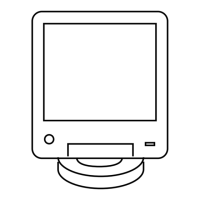
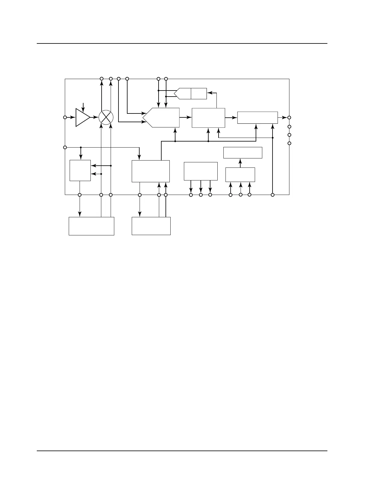
Figure 3-19. ABACUS III (AD9874) IC Functional Block Diagram from Data Sheet (UHF Range 2)
3.5.3.2.1 Second Local Oscillator (LO)
The ABACUS III IC local oscillator (LO) synthesizer controls the second LO. Signal FREF is the
16.8 MHz reference from the frequency generation unit (FGU). The second LO frequency is
107.4 MHz by default, or 111.9 MHz in special cases as necessary to avoid radio self-quieters. The
second LO signal mixes with IFIN to produce a 2.25 MHz final IF. The external VCO consists of
transistor Q5002, together with its bias and instability network and tank elements. Darlington
transistor Q5001 along with C5018 and C5050 form an active DC filter. The 2nd order loop filter is
comprised of C5044, C5045, and R5013.
3.5.3.2.2 Sampling Clock Oscillator
The ABACUS III IC sampling clock synthesizer, at Fclk=18 MHz (IF2=Fclk/8, where Fclk is the clock
rate), utilizes the clock VCO built around Q5003.
3.5.4 700–800 MHz Band
The receiver back-end (see Figure 3-16 on page 3-19) contains the following major components:
• Intermediate frequency (IF) filter
• ABACUS III IC
IFIN
FREF
-16dB
LNA
LO
Synth.
Sample Clock
Synthesizer
CLK VCO and
Loop Filter
LO VCOand
Loop Filter
Voltage
Reference
DAC AGC
ADC
Decimation
Filter
Formatting/SSI
Control Logic
f
CLK
= 13-26MHz
SPI
DOUTB
DOUTA
FS
CLKOUT
MXON
MXOP
IF2P
IF2N
GCP
GCN
LOP
IOUTL
LON
IOUTC
CLKP
CLKN
VREFP
VCM
VREFN
PC
PD
PE
SYNCB
AD9874
 Loading...