List of Figures xv
6881096C74-B May 25, 2005
List of Figures
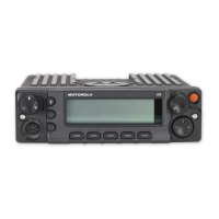
Figure 2-1. VIP Dash-Mount Configuration..............................................................................................2-2
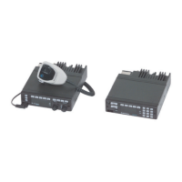
Figure 2-2. VIP Remote-Mount Configuration..........................................................................................2-3
Figure 2-3. VIP Remote-Mount Pin-Outs (Male)......................................................................................2-3
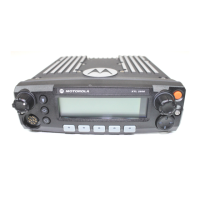
Figure 2-4. VIP Remote-Mount W3 Control-Head Configuration.............................................................2-4
Figure 2-5. VIP Remote-Mount Plus DEK Configuration .........................................................................2-5
Figure 2-6. VIP Remote-Mount Plus DEK Pin-Outs (Male) .....................................................................2-5
Figure 3-1. XTL 5000 Main Board Sections (VHF Mid Power)—Side 1 ..................................................3-2
Figure 3-2. XTL 5000 Main Board Sections (VHF Mid Power)—Side 2 ..................................................3-3
Figure 3-3. XTL 5000 Main Board Sections (VHF High Power)—Side 1.................................................3-4
Figure 3-4. XTL 5000 Main Board Sections (VHF High Power)—Side 2.................................................3-5
Figure 3-5. XTL 5000 Main Board Sections (UHF Range 1 Mid Power and UHF Range 2)—Side 1......3-6
Figure 3-6. XTL 5000 Main Board Sections (UHF Range 1 Mid Power and UHF Range 2)—Side 2......3-7
Figure 3-7. XTL 5000 Main Board Sections (UHF Range 1 High Power)—Side 1 ..................................3-8
Figure 3-8. XTL 5000 Main Board Sections (UHF Range 1 High Power)—Side 2 ..................................3-9
Figure 3-9. XTL 5000 Main Board Sections (700–800 MHz)—Side 1 ...................................................3-10
Figure 3-10. XTL 5000 Main Board Sections (700–800 MHz)—Side 2 ...................................................3-11
Figure 3-11. DC Voltage Routing Block Diagram (UHF Range 1 and UHF Range 2) .............................3-12
Figure 3-12. DC Voltage Routing Block Diagram (VHF and 700–800 MHz)............................................3-13
Figure 3-13. Receiver Block Diagram (VHF) ...........................................................................................3-14
Figure 3-14. Receiver Front-End and Back-End (UHF Range 1) ............................................................3-15
Figure 3-15. Receiver Front-End and Back-End (UHF Range 2) ............................................................3-17
Figure 3-16. Receiver Front-End and Back-End (700–800 MHz) ............................................................3-19
Figure 3-17. ABACUS III (AD9874) IC Functional Block Diagram from Data Sheet (VHF) .....................3-21
Figure 3-18. ABACUS III (AD9874) IC Functional Block Diagram from Data Sheet (UHF Range 1) ......3-22
Figure 3-19. ABACUS III (AD9874) IC Functional Block Diagram from Data Sheet (UHF Range 2) ......3-24
Figure 3-20. ABACUS III (AD9874) IC Functional Block Diagram from Data Sheet (700–800 MHz)......3-25
Figure 3-21. 50-Watt RF Power Amplifier (RFPA) Gain Stages (VHF) ....................................................3-26
Figure 3-22. 100-Watt RF Power Amplifier (RFPA) Gain Stages (VHF) ..................................................3-28
Figure 3-23. Output Network Components (VHF)....................................................................................3-29
Figure 3-24. Power Control Components (VHF)......................................................................................3-30
Figure 3-25. 40-Watt RF Power Amplifier (RFPA) Gain Stages (UHF Range 1) .....................................3-31
Figure 3-26. 100-Watt RF Power Amplifier (RFPA) Gain Stages (UHF Range 1) ...................................3-33
Figure 3-27. Output Network Components (UHF Range 1).....................................................................3-34
Figure 3-28. Power Control Components (UHF Range 1) .......................................................................3-36
Figure 3-29. 45-Watt RF Power Amplifier (RFPA) Gain Stages (UHF Range 2) .....................................3-37
Figure 3-30. Output Network Components (UHF Range 2).....................................................................3-38
Figure 3-31. Power Control Components (UHF Range 2) .......................................................................3-40
Figure 3-32. 35-Watt RF Power Amplifier (RFPA) Gain Stages (700–800 MHz) .....................................3-41
Figure 3-33. Output Network Components (700–800 MHz) ....................................................................3-42
Figure 3-34. Power Control Components (700–800 MHz).......................................................................3-44
Figure 3-35. Frequency Generation Unit Block Diagram (VHF) ..............................................................3-46
Figure 3-36. Waveform Representation During Programming of the LV Frac-N IC (VHF) ......................3-47
Figure 3-37. Frequency Generation Unit Block Diagram (UHF Range 1)................................................3-50
Figure 3-38. Waveform Representation During Programming of the LV Frac-N IC (UHF Range 1)........3-51
Figure 3-39. Frequency Generation Unit Block Diagram (UHF Range 2)................................................3-54
Figure 3-40. Waveform Representation During Programming of the LV Frac-N IC (UHF Range 2)........3-55
Figure 3-41. Frequency Generation Unit Block Diagram (700–800 MHz) ...............................................3-58
Figure 3-42. Waveform Representation During Programming of the LV Frac-N IC .................................3-59
Figure 3-43. XTL 5000 Controller Section ...............................................................................................3-63
Figure 3-44. XTL 5000 Daughtercard Module .........................................................................................3-64
 Loading...
