LPC5411x All information provided in this document is subject to legal disclaimers. © NXP Semiconductors N.V. 2018. All rights reserved.
Product data sheet Rev. 2.1 — 9 May 2018 11 of 105
NXP Semiconductors
LPC5411x
32-bit ARM Cortex-M4/M0+ microcontroller
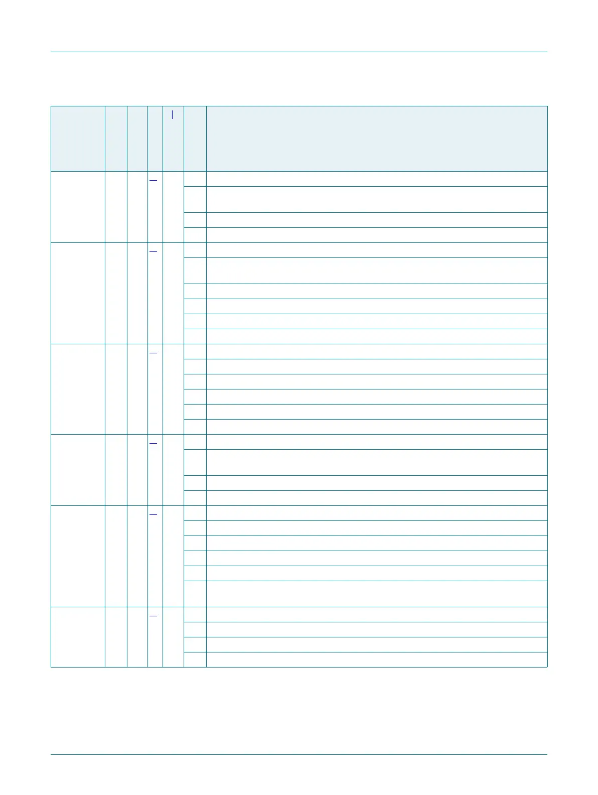
PIO0_5 C6 39
[2]
PU I/O PIO0_5 — General-purpose digital input/output pin.
I/O FC6_RXD_SDA_MOSI_DATA — Flexcomm Interface 6: USART RXD, I2C SDA,
SPI MOSI, I2S data.
O SCT0_OUT6 — SCT0 output 6. PWM output 6.
O CTimer0_MAT0 — 32-bit CTimer0 match output 0.
PIO0_6 D7 40
[2]
PU I/O PIO0_6 — General-purpose digital input/output pin.
I/O FC6_TXD_SCL_MISO_WS — Flexcomm Interface 6: USART TXD, I2C SCL, SPI
MISO, I2S WS.
R — Reserved.
O CTimer0_MAT1 — 32-bit CTimer0 match output 1.
R — Reserved.
I UTICK_CAP0 — Micro-tick timer capture input 0.
PIO0_7 D6 41
[2]
PU I/O PIO0_7 — General-purpose digital input/output pin.
I/O FC6_SCK — Flexcomm Interface 6: USART, SPI, or I2S clock.
O SCT0_OUT0 — SCT0 output 0. PWM output 0.
O CTimer0_MAT2 — 32-bit CTimer0 match output 2.
R — Reserved.
I CTimer0_CAP2 — 32-bit CTimer0 capture input 2.
PIO0_8 D5 43
[2]
PU I/O PIO0_8 — General-purpose digital input/output pin.
I/O FC2_RXD_SDA_MOSI — Flexcomm Interface 2: USART RXD, I2C SDA, SPI
MOSI.
O SCT0_OUT1 — SCT0 output 1. PWM output 1.
O CTimer0_MAT3 — 32-bit CTimer0 match output 3.
PIO0_9 E7 44
[2]
PU I/O PIO0_9 — General-purpose digital input/output pin.
I/O FC2_TXD_SCL_MISO — Flexcomm Interface 2: USART TXD, I2C SCL, SPI MISO.
O SCT0_OUT2 — SCT0 output 2. PWM output 2.
I CTimer3_CAP0 — 32-bit CTimer3 capture input 0.
R — Reserved.
I/O FC3_CTS_SDA_SSEL0 — Flexcomm Interface 3: USART CTS, I2C SDA, SPI
SSEL0.
PIO0_10 E6 45
[2]
PU I/O PIO0_10 — General-purpose digital input/output pin.
I/O FC2_SCK — Flexcomm Interface 2: USART or SPI clock.
O SCT0_OUT3 — SCT0 output 3. PWM output 3.
O CTimer3_MAT0 — 32-bit CTimer3 match output 0.
Table 4. Pin description
…continued
Symbol
49-pin
64-pin
Reset state
[1]
Type
Description
 Loading...


