LPC5411x All information provided in this document is subject to legal disclaimers. © NXP Semiconductors N.V. 2018. All rights reserved.
Product data sheet Rev. 2.1 — 9 May 2018 20 of 105
NXP Semiconductors
LPC5411x
32-bit ARM Cortex-M4/M0+ microcontroller
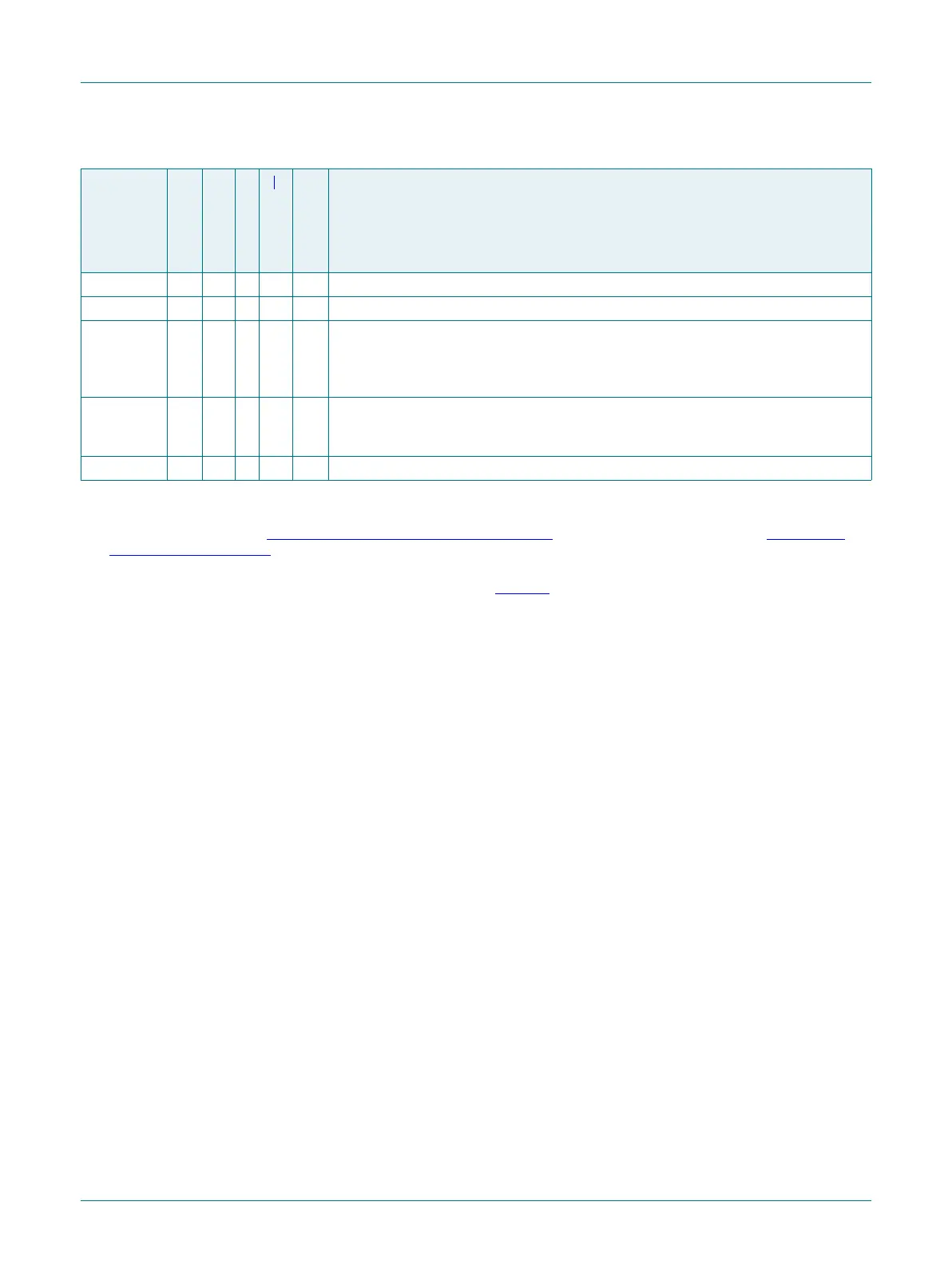
[1] PU = input mode, pull-up enabled (pull-up resistor pulls up pin to V
DD
). Z = high impedance; pull-up or pull-down disabled, AI = analog
input, I = input, O = output, F = floating. Reset state reflects the pin state at reset without boot code operation. For pin states in the
different power modes, see Section 6.2.2 “
Pin states in different power modes”. For termination on unused pins, see Section 6.2.1
“Termination of unused pins”.
[2] 5 V tolerant pad with programmable glitch filter (5 V tolerant if V
DD
present; if V
DD
not present, do not exceed 3.6 V); provides digital I/O
functions with TTL levels and hysteresis; normal drive strength. See Figure 31
. Pulse width of spikes or glitches suppressed by input
filter is from 3 ns to 16 ns (simulated value).
[3] True open-drain pin. I2C-bus pins compliant with the I2C-bus specification for I2C standard mode, I2C Fast-mode, and I2C Fast-mode
Plus. The pin requires an external pull-up to provide output functionality. When power is switched off, this pin is floating and does not
disturb the I2C lines. Open-drain configuration applies to all functions on this pin.
[4] 5 V tolerant pin providing standard digital I/O functions with configurable modes, configurable hysteresis, and analog input. When
configured as an analog input, the digital section of the pin is disabled, and the pin is not 5 V tolerant.
[5] Reset pad.5 V tolerant pad with glitch filter with hysteresis. Pulse width of spikes or glitches suppressed by input filter is from 3 ns to
20 ns (simulated value)
[6] 5 V tolerant transparent analog pad.
VREFN - 21 - - ADC negative reference voltage.
V
DDA
A4 23 - - Analog supply voltage.
V
DD
C4,
F4
8,
24,
34,
56
- - Single 1.62 V to 3.6 V power supply powers internal digital functions and I/Os.
V
SS
D4,
E4
9,
25,
55
- - Ground.
V
SSA
A3 20 - - Analog ground.
Table 4. Pin description
…continued
Symbol
49-pin
64-pin
Reset state
[1]
Type
Description

 Loading...


