LPC5411x All information provided in this document is subject to legal disclaimers. © NXP Semiconductors N.V. 2018. All rights reserved.
Product data sheet Rev. 2.1 — 9 May 2018 12 of 105
NXP Semiconductors
LPC5411x
32-bit ARM Cortex-M4/M0+ microcontroller
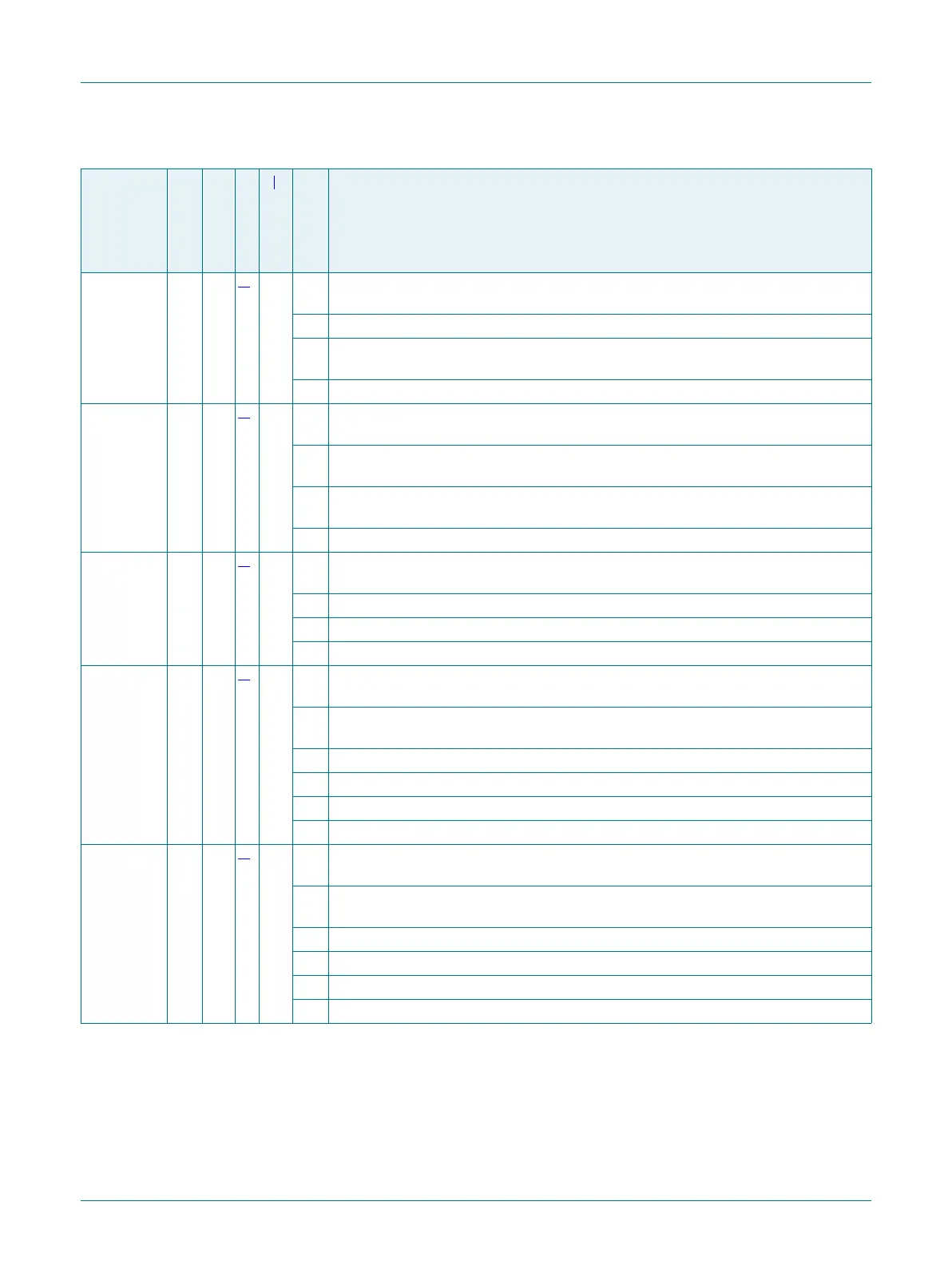
PIO0_11 E5 46
[2]
PU I/O PIO0_11 — General-purpose digital input/output pin. In ISP mode, this pin is set to
the Flexcomm 3 SPI SCK function.
I/O FC3_SCK — Flexcomm Interface 3: USART or SPI clock.
I/O FC6_RXD_SDA_MOSI_DATA — Flexcomm Interface 6: USART RXD, I2C SDA,
SPI MOSI, I2S DATA.
O CTimer2_MAT1 — 32-bit CTimer2 match output 1.
PIO0_12 F7 47
[2]
PU I/O PIO0_12 — General-purpose digital input/output pin. In ISP mode, this pin is set to
the Flexcomm 3 SPI MOSI function.
I/O FC3_RXD_SDA_MOSI — Flexcomm Interface 3: USART RXD, I2C SDA, SPI
MOSI.
I/O FC6_TXD_SCL_MISO_WS — Flexcomm Interface 6: USART TXD, I2C SCL, SPI
MISO, I2S WS.
O CTimer2_MAT3 — 32-bit CTimer2 match output 3.
PIO0_13 G7 48
[2]
PU I/O PIO0_13 — General-purpose digital input/output pin. In ISP mode, this pin is set to
the Flexcomm 3 SPI MISO function.
I/O FC3_TXD_SCL_MISO — Flexcomm Interface 3: USART TXD, I2C SCL, SPI MISO.
O SCT0_OUT4 — SCT0 output 4. PWM output 4.
O CTimer2_MAT0 — 32-bit CTimer2 match output 0.
PIO0_14/
TCK
F6 49
[2]
PU I/O PIO0_14 — General-purpose digital input/output pin. In boundary scan mode: TCK
(Test Clock In). In ISP mode, this pin is set to the Flexcomm 3 SPI SSELN0 function.
I/O FC3_CTS_SDA_SSEL0 — Flexcomm Interface 3: USART CTS, I2C SDA, SPI
SSEL0.
O SCT0_OUT5 — SCT0 output 5. PWM output 5.
O CTimer2_MAT1 — 32-bit CTimer2 match output 1.
R — Reserved.
I/O FC1_SCK — Flexcomm Interface 1: USART or SPI clock.
PIO0_15/
TDO
G6 50
[2]
PU I/O PIO0_15 — General-purpose digital input/output pin. In boundary scan mode: TDO
(Test Data Out).
I/O FC3_RTS_SCL_SSEL1 — Flexcomm Interface 3: USART RTS, I2C SCL, SPI
SSEL1.
I/O SWO — Serial wire trace output.
O CTimer2_MAT2 — 32-bit CTimer2 match output 2.
R — Reserved.
I/O FC4_SCK — Flexcomm Interface 4: USART or SPI clock.
Table 4. Pin description
…continued
Symbol
49-pin
64-pin
Reset state
[1]
Type
Description
 Loading...


