LPC5411x All information provided in this document is subject to legal disclaimers. © NXP Semiconductors N.V. 2018. All rights reserved.
Product data sheet Rev. 2.1 — 9 May 2018 13 of 105
NXP Semiconductors
LPC5411x
32-bit ARM Cortex-M4/M0+ microcontroller
SWCLK/
PIO0_16
F5 52
[2]
PU I/O PIO0_16 — General-purpose digital input/output pin.
I/O FC3_SSEL2 — Flexcomm Interface 3: SPI SSEL2.
I/O FC6_CTS_SDA_SSEL0 — Flexcomm Interface 6: USART CTS, I2C SDA, SPI
SSEL0.
O CTimer3_MAT1 — 32-bit CTimer3 match output 1.
R — Reserved.
I/O SWCLK — Serial Wire Clock. JTAG Test Clock. This is the default function after
booting.
R — Reserved.
SWDIO/
PIO0_17
G5 53
[2]
PU I/O PIO0_17 — General-purpose digital input/output pin.
I/O FC3_SSEL3 — Flexcomm Interface 3: SPI SSEL3.
I/O FC6_RTS_SCL_SSEL1 — Flexcomm Interface 6: USART RTS, I2C SCL, SPI
SSEL1.
O CTimer3_MAT2 — 32-bit CTimer3 match output 2.
R — Reserved.
I/O SWDIO — Serial Wire Debug I/O. This is the default function after booting.
PIO0_18/
TRST
G4 58
[2]
PU I/O PIO0_18 — General-purpose digital input/output pin. In boundary scan mode: TRST
(Test Reset).
I/O FC5_TXD_SCL_MISO — Flexcomm Interface 5: USART TXD, I2C SCL, SPI MISO.
O SCT0_OUT0 — SCT0 output 0. PWM output 0.
O CTimer0_MAT0 — 32-bit CTimer0 match output 0.
PIO0_19/
TDI
G3 59
[2]
PU I/O PIO0_19 — General-purpose digital input/output pin. In boundary scan mode: TDI
(Test Data In).
I/O FC5_SCK — Flexcomm Interface 5: USART or SPI clock.
O SCT0_OUT1 — SCT0 output 1. PWM output 1.
O CTimer0_MAT1 — 32-bit CTimer0 match output 1.
PIO0_20/
TMS
F3 60
[2]
PU I/O PIO0_20 — General-purpose digital input/output pin. In boundary scan mode: TMS
(Test Mode Select).
I/O FC5_RXD_SDA_MOSI — Flexcomm Interface 5: USART RXD, I2C SDA, SPI
MOSI.
I/O FC0_SCK — Flexcomm Interface 0: USART or SPI clock.
I CTimer3_CAP0 — 32-bit CTimer3 capture input 0.
PIO0_21 E3 61
[2]
PU I/O PIO0_21 — General-purpose digital input/output pin.
O CLKOUT — Clock output.
I/O FC0_TXD_SCL_MISO — Flexcomm Interface 0: USART TXD, I2C SCL, SPI MISO.
O CTimer3_MAT0 — 32-bit CTimer3 match output 0.
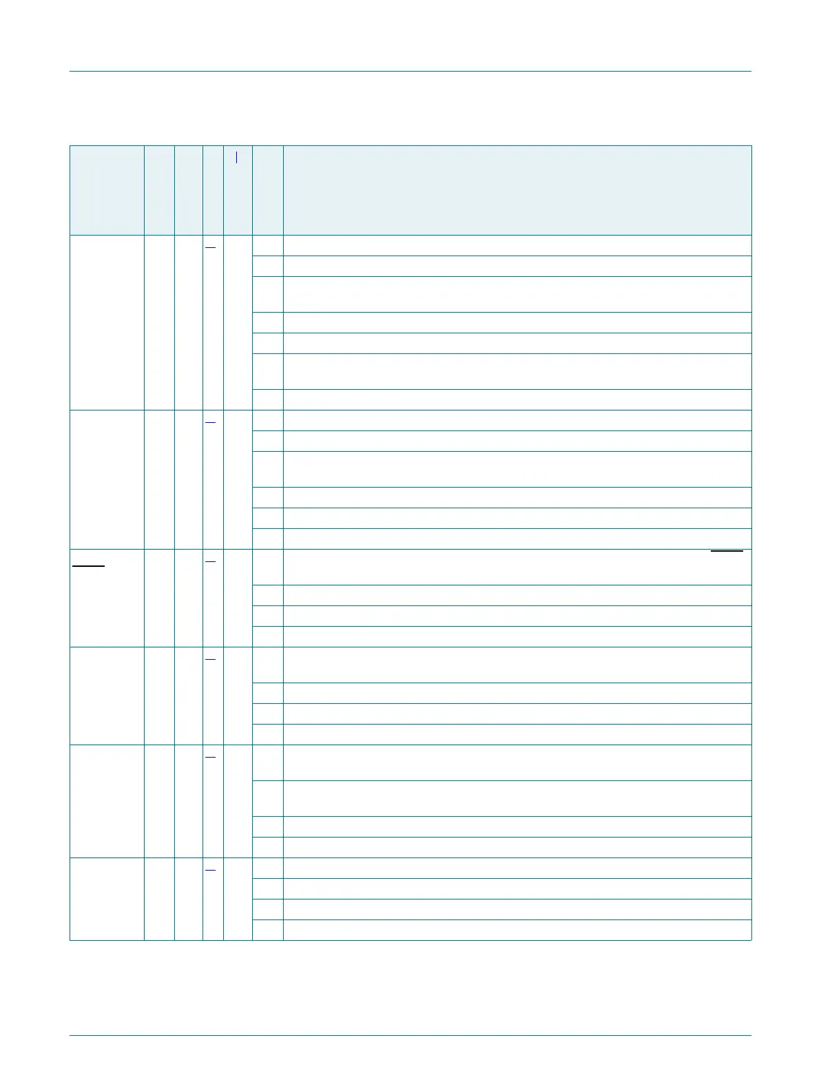
Table 4. Pin description
…continued
Symbol
49-pin
64-pin
Reset state
[1]
Type
Description

 Loading...


