LPC5411x All information provided in this document is subject to legal disclaimers. © NXP Semiconductors N.V. 2018. All rights reserved.
Product data sheet Rev. 2.1 — 9 May 2018 59 of 105
NXP Semiconductors
LPC5411x
32-bit ARM Cortex-M4/M0+ microcontroller
[1] Typical ratings are not guaranteed. The values listed are at room temperature (25 C), nominal supply voltage.
[2] Based on characterization. Not tested in production.
[3] With respect to ground.
[4] Allowed as long as the current limit does not exceed the maximum current allowed by the device.
[5] To V
SS
.
[6] The values specified are simulated and absolute values, including package/bondwire capacitance.
[7] The weak pull-up resistor is connected to the V
DD
rail and pulls up the I/O pin to the V
DD
level.
[8] The value specified is a simulated value, excluding package/bondwire capacitance.
[9] Without 33 Ω 2 % series external resistor.
[10] The parameter values specified are simulated and absolute values.
[11] With 33 Ω 2 % series external resistor.
[12] With 15 KΩ 5 % resistor to V
SS
.
[13] With 1.5 KΩ 5% resistor to 3.6 V external pull-up.
[14] Guaranteed by design, not tested in production.
Pin capacitance
C
io
input/output capacitance I
2
C-bus pins
[8]
--6.0pF
pins with digital functions only
[6]
--2.0pF
Pins with digital and analog
functions
[6]
--7.0pF
Table 20. Static characteristics: pin characteristics …continued
T
amb
=
40
C to +105
C, unless otherwise specified. 1.62 V
V
DD
3.6 V unless otherwise specified. Values tested in
production unless otherwise specified.
Symbol Parameter Conditions Min Typ
[1]
Max Unit
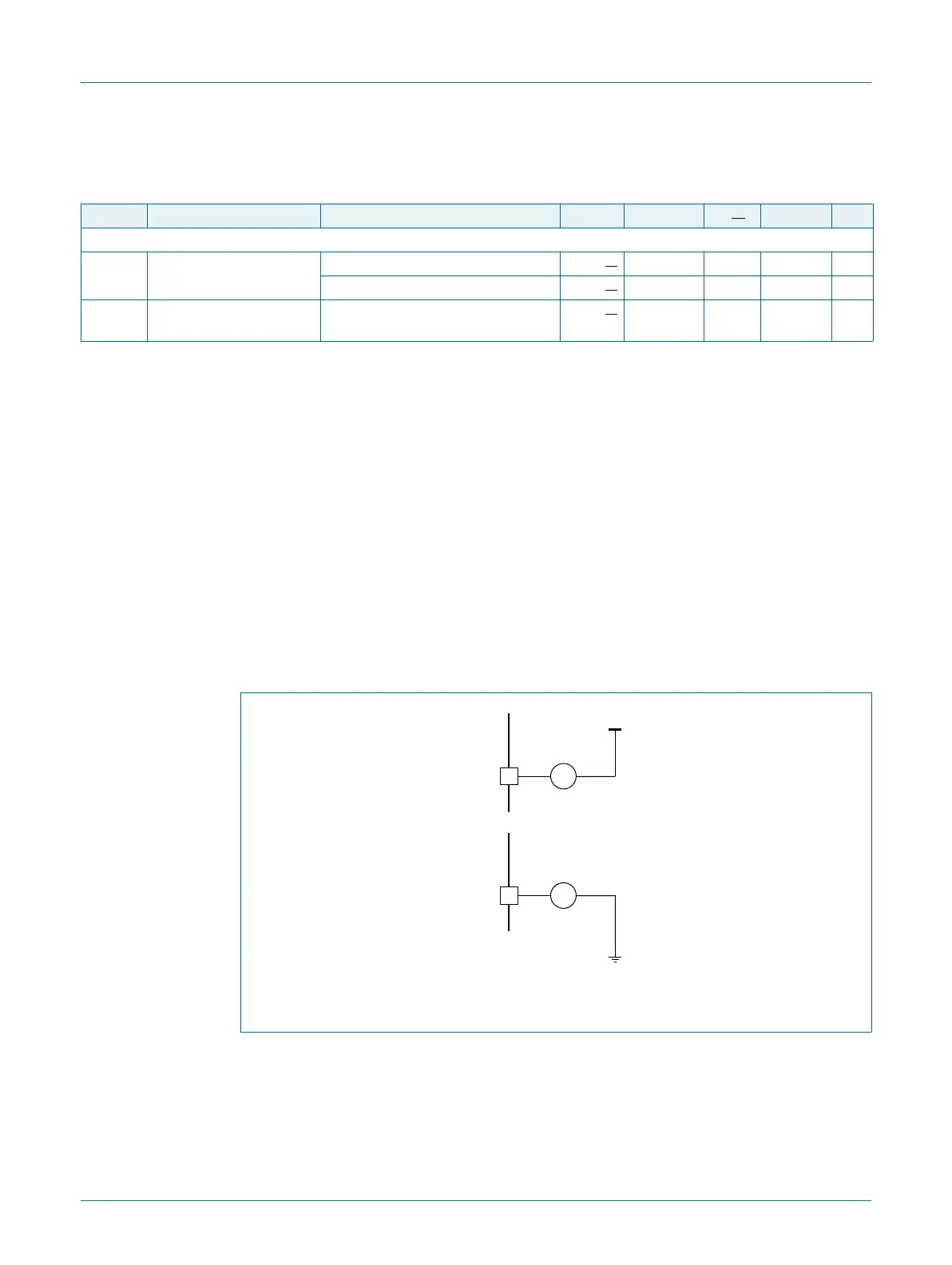
Fig 13. Pin input/output current measurement
aaa-010819
+
-
pin PIO0_n
I
OH
Ipu
-
+
pin PIO0_n
I
OL
I
pd
V
DD
A
A

 Loading...


