PUMA T2
Technical Handbook
Technical description
Page 40 OTE Proprietary information
P/N: 779-0306/01
Revision 03
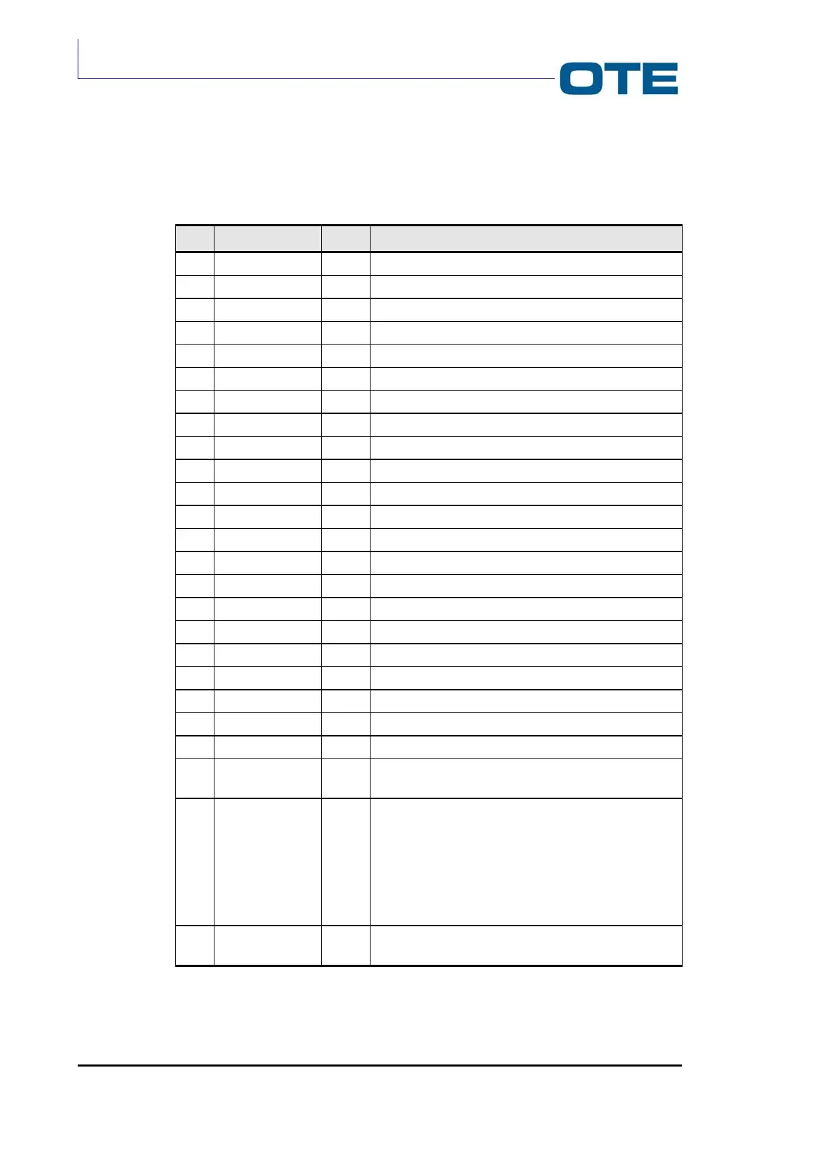
Tab. 2.2 shows the interface signals allocation on the I/F RT connector and their
meaning.
Tab. 2.2: I/F RT connector interface signals
Pin Name Type Description
1 ITX OUT Base band I signal from CMX980 to the transmitter
2 QTX OUT Base band Q signal from CMX980 to the transmitter
3
IRX
IN
Base band I signal from the receiver to CMX980
4
QRX
IN
Base band Q signal from the receiver to CMX980
5
IF
IN
Base band I signal from the transmitter to CMX980
6 QF IN Base band Q signal from the transmitter to CMX980
7 RX-GATE OUT From FPGA to RT
8 ON/OFF OUT On/off to RT
9
MANT-AL
OUT
Equipment maintained power supply to RT
10 SD OUT Shut down towards RT (transmitter)
11 PRES-AL OUT Internal/external power supply to RT
12
RX-ON
OUT
From FPGA to RT
13 TX-ON OUT From FPGA to RT
14 TX-GATE OUT From FPGA to RT
15 HDATASER OUT Data for serial output from FPGA
16 HCKSER OUT Serial clock for 3 DAC quad, SINT and EEPROM
17 HENSYNT OUT Enable serial on synthesizer
18 HENDAC OUT Enable serial for the 3 DACs on radio card
19 HENEEPROM OUT Enable EEPROM serial on radio card
20 SERDATAIN IN EEPROM reading serial data on radio card
21 VBI P Battery voltage to digital board
22 VBI P Battery voltage to digital board
23 GND P GND on connector; the common battery analogue
digital mass point
24 Fref IN Reference frequency from radio card to base band
board.
PUMA T2-400: Fref = 14.4 MHz
PUMA T2-430: Fref = 14.4 MHz
PUMA T2-470: Fref = 19.8 MHz
PUMA T2-870: Fref = 14.4 MHz
25 GND P GND on connector; we have the common battery
analogue digital mass point.