PUMA T2
Technical Handbook
Technical description
Page 44 OTE Proprietary information
P/N: 779-0306/01
Revision 03
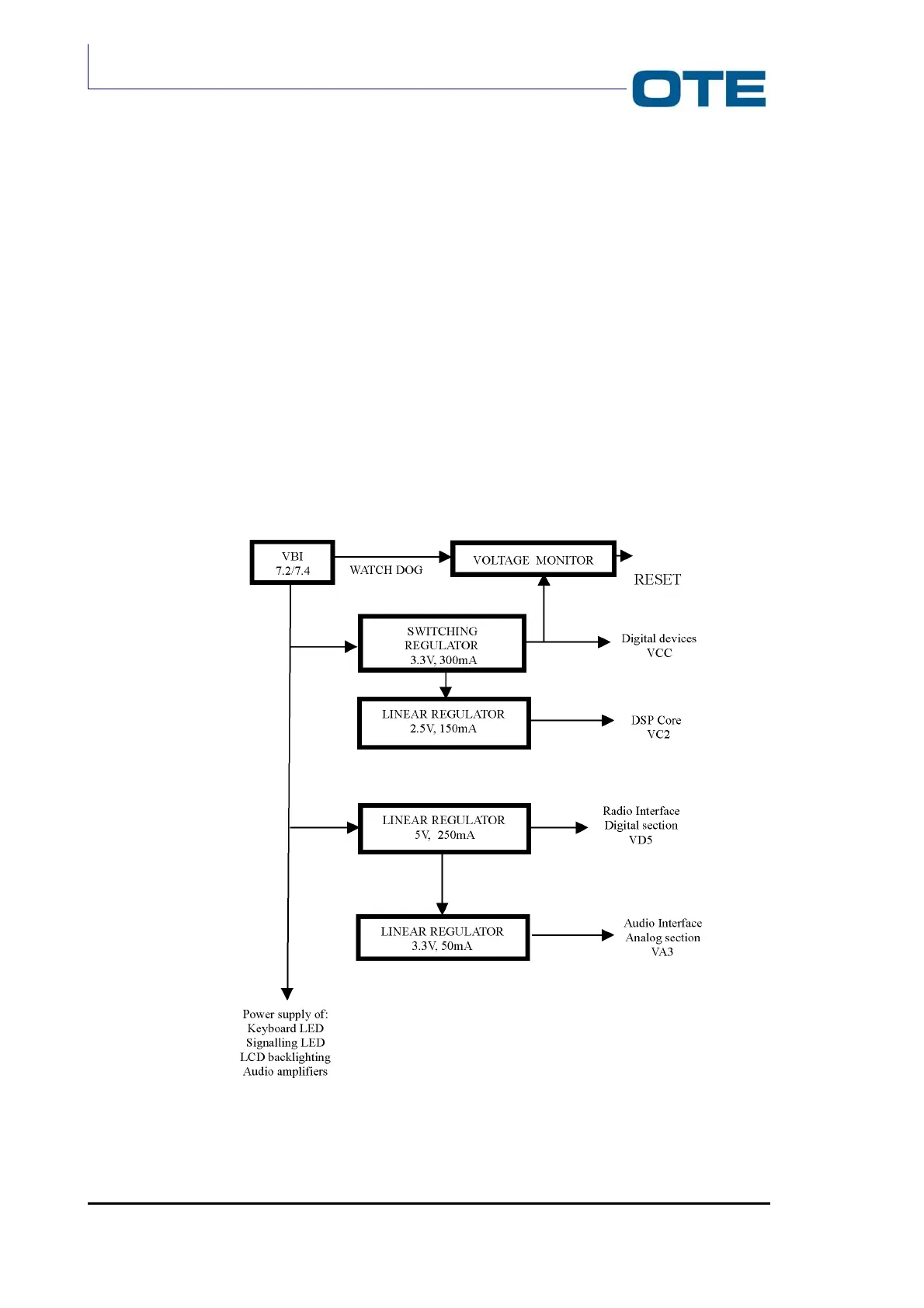
2.5 POWER SUPPLY
The purpose of the power supply, whose block diagram is shown in Fig. 2.2, is to
supply the voltages for the base band circuits, beginning from the VBI general
power supply voltage (7.2 V).
The following voltages are required by the Base Band:
• VCC, 3.3 V for the 3.3 V digital logic circuits
• VA3, 3.3 V for the 3.3 V analog circuits
• VD5, 5.0 V for the 5 V digital circuits
• VC2, 2.5 V to feed the Digital Signal Processor
The VCC power supply voltage level and the microprocessor switching rate are
regularly tested by the voltage monitor device (Fig. 2.2).
Fig. 2.2: Power supply functional block diagram