SCK
(CPOL=’0’)
MISO
XSS
MOSI
0 1 2 3 4 5 6 7 8 9 10 11 20 21 22 23 24 25 26 27 28 29 30 31
15 14 13 12 3 2 1 0
7 6 5 4 3 2 1 0
0 0 0 0 0 0 1 1
Instruction 16-bit Address
Data Byte 1
High-Impedance
“don’t care”
7 6 5 4 3 2 1 0
Data Byte n
SCK
(CPOL=’0’)
MISO
XSS
MOSI
7 6 5 4 3 2 1 0
Data Byte 2
7 6 5 4 3 2 1 0
Data Byte 3
32 33 34 35 36 37 38 39 40 41 42 43 44 45 46 47
“don’t care”
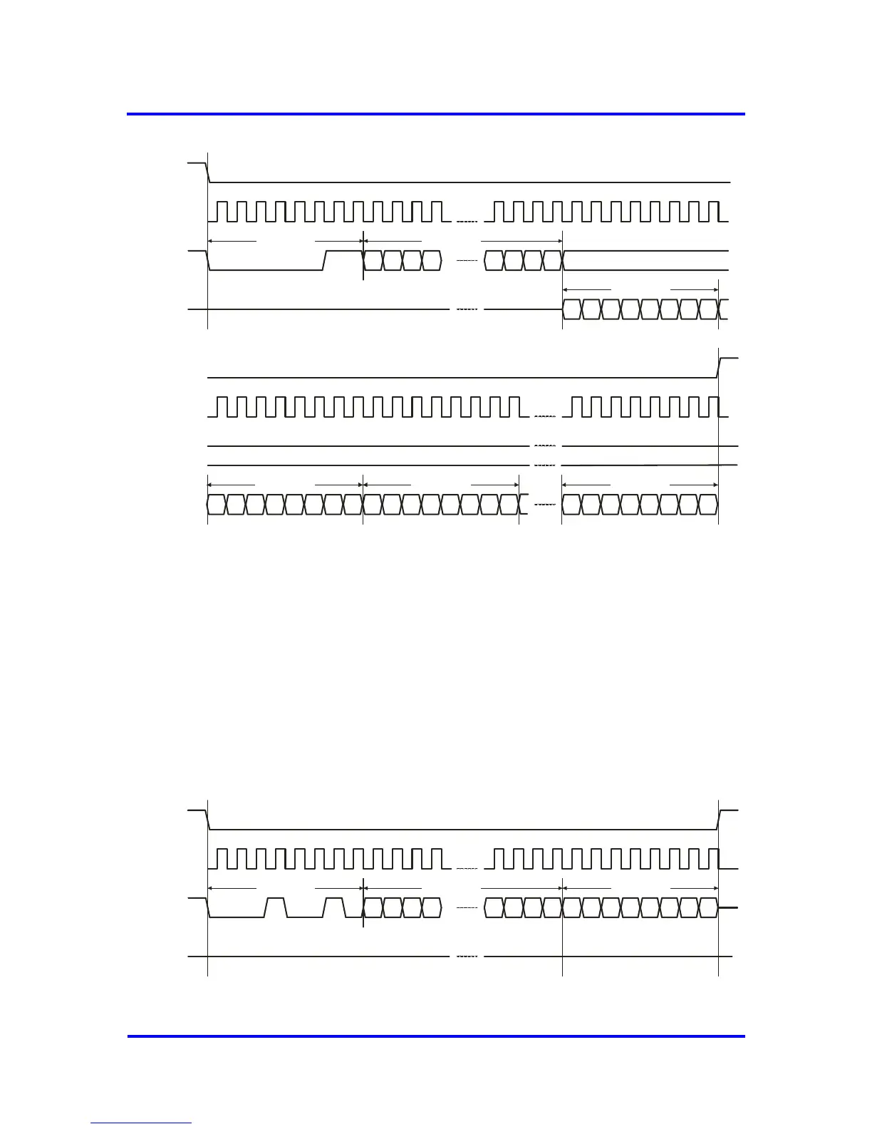
Figure 8-8: READ ARRAY Sequence
WRITE BYTE Sequence
The VPC3+S is selected by pulling XSS low. The 8-bit WRITE BYTE
instruction is transmitted to the device followed by the 16-bit address, with
the four MSBs of the address being “don’t care” bits (in case of 2 kB RAM
mode the five MSBs of the address are “don’t care”).
After the correct WRITE BYTE instruction and address are sent, the data
byte is shifted in on the MOSI pin. Once 8 SCK clock pulses are received
the sampled data byte is written to the selected address. Providing more
SCK clock pulses does not affect the VPC3+S. The write operation is
terminated by raising the XSS pin.
SCK
(CPOL=’0’)
MISO
XSS
MOSI
0 1 2 3 4 5 6 7 8 9 10 11 20 21 22 23 24 25 26 27 28 29 30 31
15 14 13 12 3 2 1 0 7 6 5 4 3 2 1 00 0 0 1 0 0 1 0
Instruction 16-bit Address Data In
High-Impedance