Copyright © profichip GmbH, 2012
Note:
When reading from the Control Parameter memory (address 0x000 to
address 0x015) only the READ BYTE instruction may be used.
Otherwise an unintended read operation to the subsequent memory
location will occur leading to an unpredictable behavior of the VPC3+S.
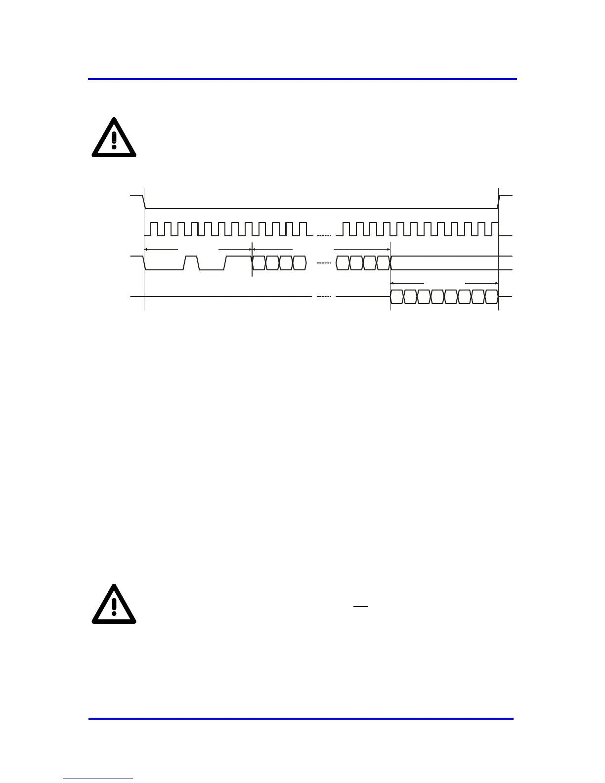
Figure 8-7: READ BYTE Sequence
READ ARRAY Sequence
The device is selected by pulling XSS low. The 8-bit READ BYTE instruc-
tion is transmitted to the VPC3+S followed by the 16-bit address, with the
four MSBs of the address being “don’t care” bits (in case of 2 kB RAM
mode the five MSBs of the address are “don’t care”).
After the correct READ ARRAY instruction and address are sent, the data
byte stored in the memory at the selected address is shifted out on the
MISO pin. After additional 8 SCK pulses the complete first data byte has
been sent. The data byte stored in the memory at the next address can be
read sequentially by continuing to provide clock pulses. The internal Ad-
dress Pointer is automatically incremented to the next higher address after
each byte of data is shifted out. When the highest address is reached
(0x7FF in case of 2 kB RAM mode or 0xFFF in 4 kB mode), the address
counter rolls over to address 0x000 allowing the read cycle to be continued
indefinitely. The read operation is terminated by raising the XSS pin (Figure
8-8).
Note:
The SPI instruction READ ARRAY may not be used when reading from the
Control Parameter memory (address 0x000 to address 0x015).
Otherwise (due to the auto-increment mechanism of the READ ARRAY
instruction) an unintended read operation to the subsequent memory loca-
tion will occur leading to an unpredictable behavior of the VPC3+S.