5G Module Series
RM500Q-AE&RM502Q-AE Hardware Design
RM500Q-AE&RM502Q-AE_Hardware_Design 50 / 86
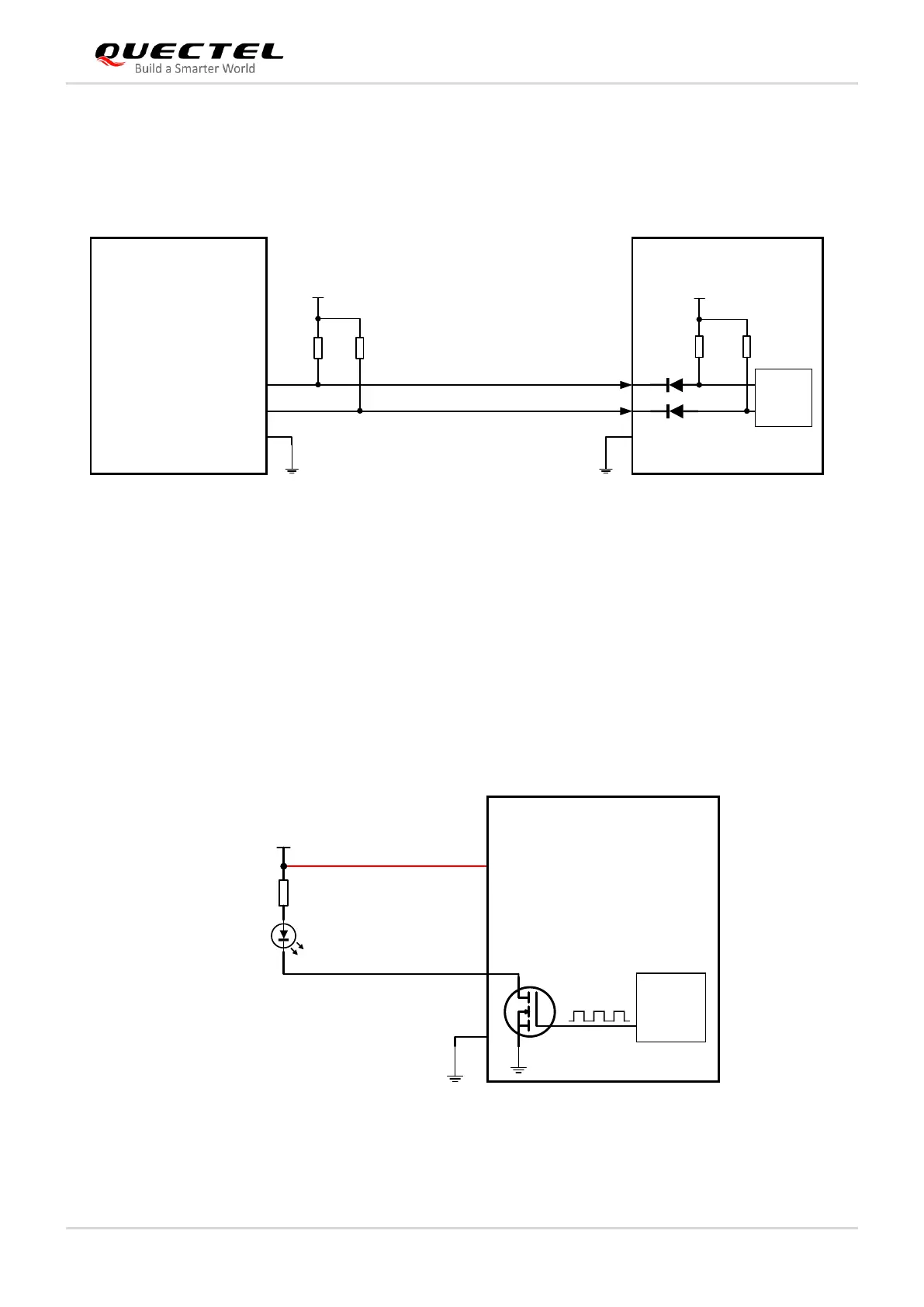
A simple level shifter based on diodes is used on W_DISABLE1# pin and W_DISABLE2# pin which are
pulled up to a 1.8 V voltage in the module, as shown in the following figure. So, the control signals (GPIO)
of the host device could be at 1.8 V or 3.3 V voltage level. W_DISABLE1# and W_DISABLE2# are active
LOW signals, and a reference circuit is shown as below.
Host Module
W_DISABLE2#
W_DISABLE1#
BB
GPIO
GPIO
26
8
VDD 1.8V
R3
10k
R4
10k
NOTE: The voltage level of VCC_IO_HOST could be 1.8 V or 3.3 V typically.
VCC_IO_HOST
R1
100k
R2
100k
Figure 24: W_DISABLE1# and W_DISABLE2# Reference Circuit
4.5.3. WWAN_LED#
The WWAN_LED# signal is used to indicate RF status of the module, and its sink current is up to 10 mA.
To reduce current consumption of the LED, a current-limited resistor must be placed in series with the
LED, as illustrated in the figure below. The LED is ON when the WWAN_LED# signal is at low level.
Module
WWAN_LED#
PMIC
10
VCC(Typ. 3.7V)
R1
330 Ω
LED1
2, 4
70,72,74
VCC
Figure 25: WWAN_LED# Reference Circuit
 Loading...