EasyManuals Logo

Quectel 5G Module Series Hardware Design

Quectel 5G Module Series
87 pages
To Next Page IconTo Next Page
To Previous Page IconTo Previous Page
Page #54 background imageLoading...
Page #54 background image
5G Module Series
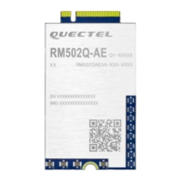
RM500Q-AE&RM502Q-AE Hardware Design
RM500Q-AE&RM502Q-AE_Hardware_Design 53 / 86
4.7. Antenna Tuner Control Interface*
ANTCTL[1:2] and RFFE interface are used for antenna tuner control and should be routed to an
appropriate antenna control circuit. More details about the interface will be added in the future version of
this document.
Table 27: Pin Definition of Antenna Tuner Control Interface
1)
If this function is required, please contact Quectel for more details.
4.8. Configuration Pins
The module provides four configuration pins, which are defined as below.
Table 28: Configuration Pins List of M.2 Specification
62
COEX_RXD*
DI, PD
LTE/WLAN coexistence receive
1.8 V
64
COEX_TXD*
DO, PD
LTE/WLAN coexistence transmit
1.8 V
Pin No.
Pin Name
I/O
Description
DC Characteristics
56
RFFE_CLK
1)
DO, PD
Used for external
MIPI IC control
1.8 V
58
RFFE_DATA
1)
DIO, PD
1.8 V
65
RFFE_VIO_1V8
1)
PO
Power supply for
antenna tuner
1.8 V.
Maximum output current: 50 mA
61
ANTCTL1*
DO, PD
Antenna GPIO
Control
1.8 V
63
ANTCTL2*
DO, PD
1.8 V
Config_0
(Pin 21)
Config_1
(Pin 69)
Config_2
(Pin 75)
Config_3
(Pin 1)
Module Type and
Main Host Interface
Port
Configuration
NC
GND
NC
NC
Quectel defined
2
NOTE

Table of Contents

Other manuals for Quectel 5G Module Series

Questions and Answers:

Question and Answer IconNeed help?

Do you have a question about the Quectel 5G Module Series and is the answer not in the manual?

Quectel 5G Module Series Specifications

General IconGeneral
BrandQuectel
Model5G Module Series
CategoryMotherboard
LanguageEnglish

Related product manuals