R8C/20 Group, R8C/21 Group 13. Watchdog Timer
Rev.2.00 Aug 27, 2008 Page 114 of 458
REJ09B0250-0200
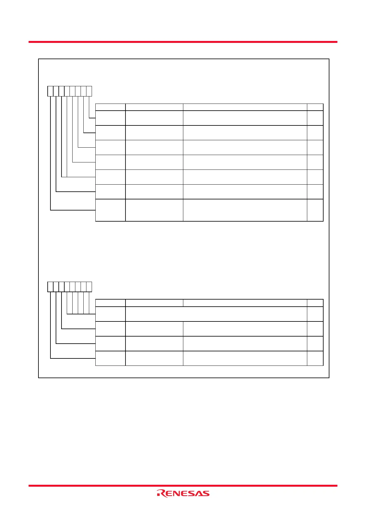
Figure 13.2 Registers OFS and WDC
Watchdog Timer Control Register
Symbol Address After Reset
WDC
000Fh 00X11111b
Bit Symbol Bit Name Function RW
—
(b5)
Reserved bits Set to 0.
When read, the content is undefined.
RW
RW
High-order bits of w atchdog timer
b3 b2 b1 b0
—
(b4-b0)
RO
b7 b6 b5 b4
00
RW
WDC7
—
(b6)
Reserved bits Set to 0
Prescaler select bit 0 : Divide-by-16
1 : Divide-by-128
Option Function Select Register
(1)
Symbol Address Before Shipment
OFS
0FFFFh FFh
(3)
Bit Symbol Bit Name Function RW
Reserved bit
NOTES:
1.
2.
3.
b7 b6 b5 b4 b3 b2 b1 b0
11 1
—
(b1)
Set to 1
RW
WDTON
Watchdog timer start
select bit
0 : Starts w atchdog timer automatically after reset
1 : Watchdog timer is inactive after reset
RW
ROMCR
ROM code protect
disabled bit
0 : ROM code protect disabled
1 : ROMCP1 enabled
RW
ROMCP1
ROM code protect bit 0 : ROM code protect enabled
1 : ROM code protect disabled
RW
RW
—
(b5-b4)
Reserved bits Set to 1
RW
If the block including the OFS register is erased, FFh is set to the OFS register.
To use the pow er-on reset, set the LVD1ON bit to 0 (voltage monitor 1 reset enabled after reset).
LVD1ON
Voltage detection circuit
start bit
(2)
0 : Voltage monitor 1 reset enabled after reset
1 : Voltage monitor 1 reset disabled after reset
RW
The OFS register is on the flash memory. Write to the OFS register w ith a program. After w riting is completed, do not
w rite additions to the OFS register.
CSPROINI
Count source protect
mode after reset select
bit
0 : Count source protect mode enabled after reset
1 : Count source protect mode disabled after reset
 Loading...