R8C/20 Group, R8C/21 Group 14. Timers
Rev.2.00 Aug 27, 2008 Page 186 of 458
REJ09B0250-0200
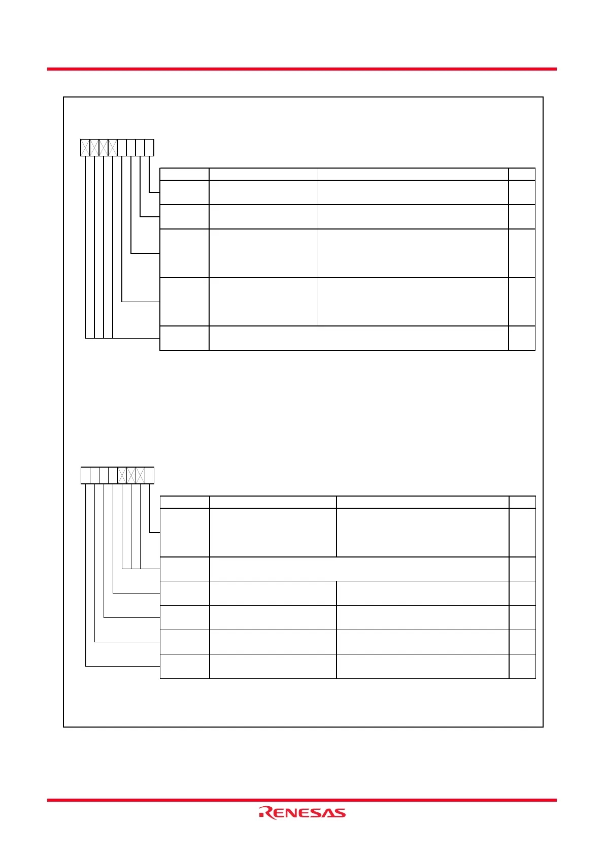
Figure 14.48 Registers TRDSTR and TRDMR in Output Compare Function
Timer RD Start Register
(1)
Symbol Address After Reset
TRDSTR
0137h 11111100b
Bit Symbol Bit Name Function RW
NOTES:
1.
2.
3.
4.
5.
Set the TRDSTR register using the MOV instruction (do not use the bit handling instruction). Refer to
14.3.12.1
TRDSTR Re gis te r
of
Notes on Timer RD
.
TRD0 count operation select
bit
0 : Count stops at the compare match w ith
the TRDGRA0 register after the count clear
1 : Count continues at the compare match w ith
the TRDGRA0 register after the count clear
CSEL0 RW
RW
TRD1 count operation select
bit
0 : Count stops at the compare match w ith
the TRDGRA1 register after the count clear
1 : Count continues at the compare match w ith
the TRDGRA1 register after the count clear
—
—
(b7 - b4)
RW
TSTART1 RW
TRD1 count start flag
(5)
0 : Count stops
(3)
1 : Count starts
TRD0 count start flag
(4)
0 : Count stops
(2)
1 : Count starts
Nothing is assigned. If necessary, set to 0.
When read, the content is 1.
b7 b6 b5 b4 b3 b2
CSEL1
b1 b0
TSTART0
When the CSEL0 bit is set to 1, w rite 0 to the TSTART0 bit.
When the CSEL1 bit is set to 1, w rite 0 to the TSTART1 bit.
When the CSEL0 bit is set to 0 and generating the compare match signal (TRDIOA0), this bit is set to 0 (count stops).
When the CSEL1 bit is set to 0 and generating the compare match signal (TRDIOA1), this bit is set to 0 (count stops).
Timer RD Mode Register
Symbol Address After Reset
TRDMR
0138h 00001110b
Bit Symbol Bit Name Function RW
NOTE:
1. When selecting 0 (change the TRDGRji register output pin) by the IOj3 (j = C or D) bit in the TRDIORCi (i = 0 or 1)
register, set the BFji bit in the TRDMR register to 0.
RWBFC1
BFD1
TRDGRD1 register function
selection bit
(1)
0 : General register
1 : Buffer register of TRDGRB1 register
RW
TRDGRC0 register function
selection bit
(1)
0 : General register
1 : Buffer register of TRDGRA0 register
BFC0 RW
RW
TRDGRD0 register function
selection bit
(1)
0 : General register
1 : Buffer register of TRDGRB0 register
TRDGRC1 register function
selection bit
(1)
0 : General register
1 : Buffer register of TRDGRA1 register
RW
—
(b3 - b1)
—
Timer RD synchronous bit 0 : TRD0 and TRD1 registers
operate independently
1 : TRD0 and TRD1 registers
operate synchronously
Nothing is assigned. If necessary, set to 0.
When read, the content is 1.
b7 b6 b5 b4 b3 b2
BFD0
b1 b0
SYNC
 Loading...