R8C/20 Group, R8C/21 Group 14. Timers
Rev.2.00 Aug 27, 2008 Page 188 of 458
REJ09B0250-0200
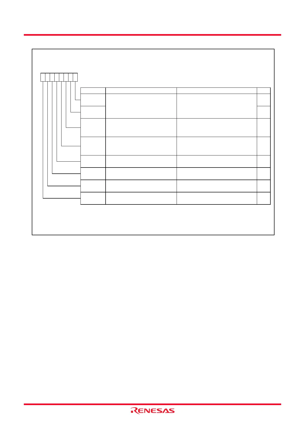
Figure 14.50 TRDFCR Register in Output Compare Function
Timer RD Function Control Register
Symbol Address After Reset
TRDFCR
013Ah 10000000b
Bit Symbol Bit Name Function RW
NOTES:
1.
2. When bits CMD1 to CMD0 are set to 00b (timer mode, PWM mode, or PWM3 mode), the setting of the PWM3 bit is
enabled.
b3 b2
OLS1
b1 b0
001
b7 b6 b5 b4
RW
CMD1 RW
Combination mode selection bit
(1)
Set to 00b (timer mode, PWM mode, or
PWM3 mode) in the output compare
function.
CMD0
Normal-phase output level selection
bit (in reset synchronous PWM mode
or complementary PWM mode)
This bit is disabled in the output compare
function.
Set bits CMD1 to CMD0 w hen both the TSTART0 and TSTART1 bits in the TRDSTR register are set to 0 (count stops).
OLS0 RW
RW
Counter-phase output level selection
bit (in reset synchronous PWM mode
or complementary PWM mode)
This bit is disabled in the output compare
function.
A/D trigger enable bit
(in complementary PWM mode)
This bit is disabled in the output compare
function.
RW
PWM3 RW
ADTRG
ADEG
A/D trigger edge selection bit
(in complementary PWM mode)
This bit is disabled in the output compare
function.
RW
PWM3 mode selection bit
(2)
Set this bit to 1 (other than PWM3 mode) in
the output compare function.
STCLK
External clock input selection bit 0 : External clock input disabled
1 : External clock input enabled
RW
 Loading...