R8C/20 Group, R8C/21 Group 14. Timers
Rev.2.00 Aug 27, 2008 Page 192 of 458
REJ09B0250-0200
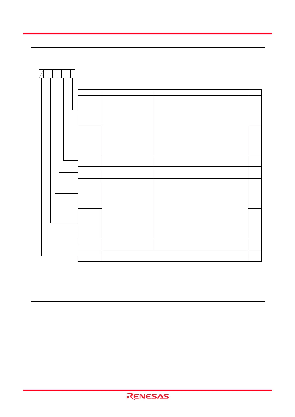
Figure 14.54 Registers TRDIORA0 to TRDIORA1 in Output Compare Function
Timer RD I/O Control Register Ai (i = 0 or 1)
Symbol Address After Reset
TRDIORA0
TRDIORA1
0141h
0151h
10001000b
10001000b
Bit Symbol Bit Name Function RW
NOTES:
1.
2.
Input capture input sw itch
bit
Set to 1
RW
Nothing is assigned. If necessary, set to 0.
When read, the content is 1.
RW
RW
IOA 1
IOA 0
TRDGRA control bit
b1 b0
0 0 : Disable pin output by the compare match
(TRDIOAi pin functions as programmable
I/O port)
0 1 : “L” output by the compare match in
the TRDGRAi register
1 0 : “H” output by the compare match in
the TRDGRAi register
1 1 : Toggle output by the compare match
in the TRDGRAi register
TRDGRA mode selection
bit
(1)
Set to 0 (output compare) in the output compare
function
RW
IOB2 RW
TRDGRB control bit
b5 b4
0 0 : Disable pin output by the compare match
(TRDIOBi pin functions as programmable
I/O port)
0 1 : “L” output by the compare match
in the TRDGRBi register
1 0 : “H” output by the compare match
in the TRDGRBi
1 1 : Toggle output by the compare match
in the TRDGRBi register
b7 b6 b5 b4
0
b3 b2
IOA 3
b1 b0
10
IOA 2
When selecting 1 (The TRDGRDi register is used as a buffer register of TRDGRBi register) for this bit by the BFDi bit
in the TRDMR register, set the IOD2 bit in the TRDIORCi register to the same as the IOB2 bit in the TRDIORAi register.
—
IOB0
IOB1 RW
When selecting 1 (The TRDGRCi register is used as a buffer register of the TRDGRAi register) for this bit by the BFCi
bit in the TRDMR register, set the IOC2 bit in the TRDIORCi register to the same as the IOA2 bit in the TRDIORAi
register.
TRDGRB mode selection
bit
(2)
Set to 0 (output compare) in the output compare
function
RW
—
(b7)
 Loading...