R8C/20 Group, R8C/21 Group 14. Timers
Rev.2.00 Aug 27, 2008 Page 193 of 458
REJ09B0250-0200
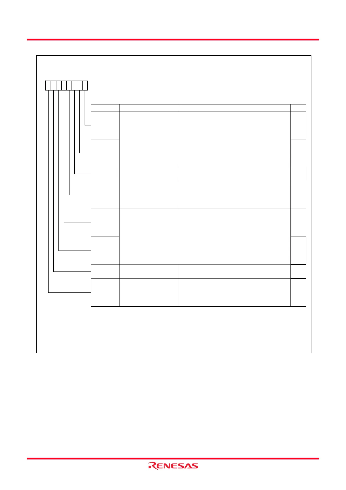
Figure 14.55 Registers TRDIORC0 to TRDIORC1 in Output Compare Function
Timer RD I/O Control Register Ci (i = 0 or 1)
Symbol Address After Reset
TRDIORC0
TRDIORC1
0142h
0152h
10001000b
10001000b
Bit Symbol Bit Name Function RW
NOTES:
1.
2. When selecting 1 (The TRDGRDi register is used as a buffer register of TRDGRBi register) for this bit by the BFDi bit
in the TRDMR register, set the IOD2 bit in the TRDIORCi register to the same as the IOB2 bit in the TRDIORAi register.
TRDGRC mode selection
bit
(1)
Set to 0 (output compare) in the output compare
function
RW
TRDGRC register function
selection bit
(1)
0 : TRDIOA output register
(Refer to
14.3.6.1 Changing Output Pins in
Registers TRDGRCi (i = 0 or 1) and TRDGRDi
)
1 : General register or buffer register
RW
IOD0
IOD1
RW
RW
RW
IOC1
IOC0
TRDGRC control bit
b1 b0
0 0 : Disable pin output by the compare match
0 1 : “L” output by the compare match in
the TRDGRCi register
1 0 : “H” output by the compare match in
the TRDGRCi register
1 1 : Toggle output by the compare match
in the TRDGRCi register
RW
TRDGRD control bit
b5 b4
0 0 : Disable pin output by the compare match
0 1 : “L” output by the compare match in
the TRDGRDi register
1 0 : “H” output by the compare match in
the TRDGRDi register
1 1 : Toggle output by the compare match
in the TRDGRDi register
b7 b6 b5 b4
0
b3 b2
IOC3
b1 b0
0
IOC2
When selecting 1 (The TRDGRCi register is used as a buffer register of the TRDGRAi register) for this bit by the BFCi
bit in the TRDMR register, set the IOC2 bit in the TRDIORCi register to the same as the IOA2 bit in the TRDIORAi
register.
TRDGRD mode selection
bit
(2)
Set to 0 (output compare) in the output compare
function
IOD3
IOD2 RW
TRDGRD register function
selection bit
0 : TRDIOB output register
(Refer to
14.3.6.1 Changing Output Pins in
Registers TRDGRCi (i = 0 or 1) and TRDGRDi
)
1 : General register or buffer register
RW
 Loading...