R8C/20 Group, R8C/21 Group 14. Timers
Rev.2.00 Aug 27, 2008 Page 196 of 458
REJ09B0250-0200
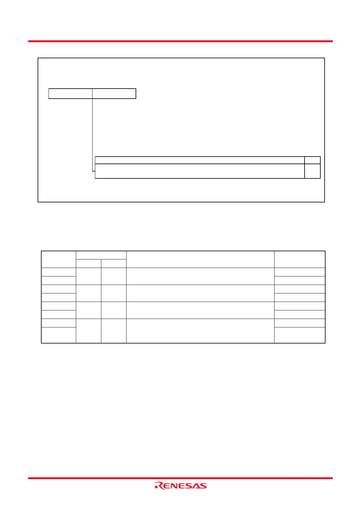
Figure 14.59 Registers TRDGRAi, TRDGRBi, TRDGRCi and TRDGRDi in Output Compare Function
The following registers are disabled in the output compare function:
TRDDF0, TRDDF1, TRDPOCR0 and TRDPOCR1
i = 0 or 1, j = either A, B, C or D
BFji: Bit in TRDMR register IOj3: Bit in TRDIORCi register
Table 14.26 TRDGRji Register Functions in Output Compare Function
Register
Setting
Register Function
Output-Compare
Output Pin
BFji IOj3
TRDGRAi −−General register. Write the compare value. TRDIOAi
TRDGRBi TRDIOBi
TRDGRCi 0 1 General register. Write the compare value. TRDIOCi
TRDGRDi TRDIODi
TRDGRCi 1 1 Buffer register. Write the next compare value
(refer to 14.3.2 Buffer Operation.)
TRDIOAi
TRDGRDi TRDIOBi
TRDGRCi 0 0 TRDIOAi output control (refer to 14.3.6.1 Changing
Output Pins in Registers TRDGRCi (i = 0 or 1) and
TRDGRDi.)
TRDIOAi
TRDGRDi TRDIOBi
Timer RD General Register Ai, Bi, Ci and Di (i = 0 or 1)
(1)
Symbol Address After Reset
TRDGRA0
TRDGRB0
TRDGRC0
TRDGRD0
TRDGRA1
TRDGRB1
TRDGRC1
TRDGRD1
0149h-0148h
014Bh-014Ah
014Dh-014Ch
014Fh-014Eh
0159h-0158h
015Bh-015Ah
015Dh-015Ch
015Fh-015Eh
FFFFh
FFFFh
FFFFh
FFFFh
FFFFh
FFFFh
FFFFh
FFFFh
RW
NOTE:
1.
RW
Function
Refer to
Table 14.26 TRDGRji Register Functions in Output Compare Function
Access the TRDGRAi to TRDGRDi registers in 16-bit units. Do not access them in 8-bit units.
b0b7
(b8)
b0
(b15)
b7
 Loading...