R8C/20 Group, R8C/21 Group 14. Timers
Rev.2.00 Aug 27, 2008 Page 238 of 458
REJ09B0250-0200
i = 0 or 1, j = either A, B, C or D
Table 14.33 PWM3 Mode Specifications
Item Specification
Count Sources f1, f2, f4, f8, f32, fOCO40M
Count Operations The TRD0 register is incremented. (The TRD1 is not used.)
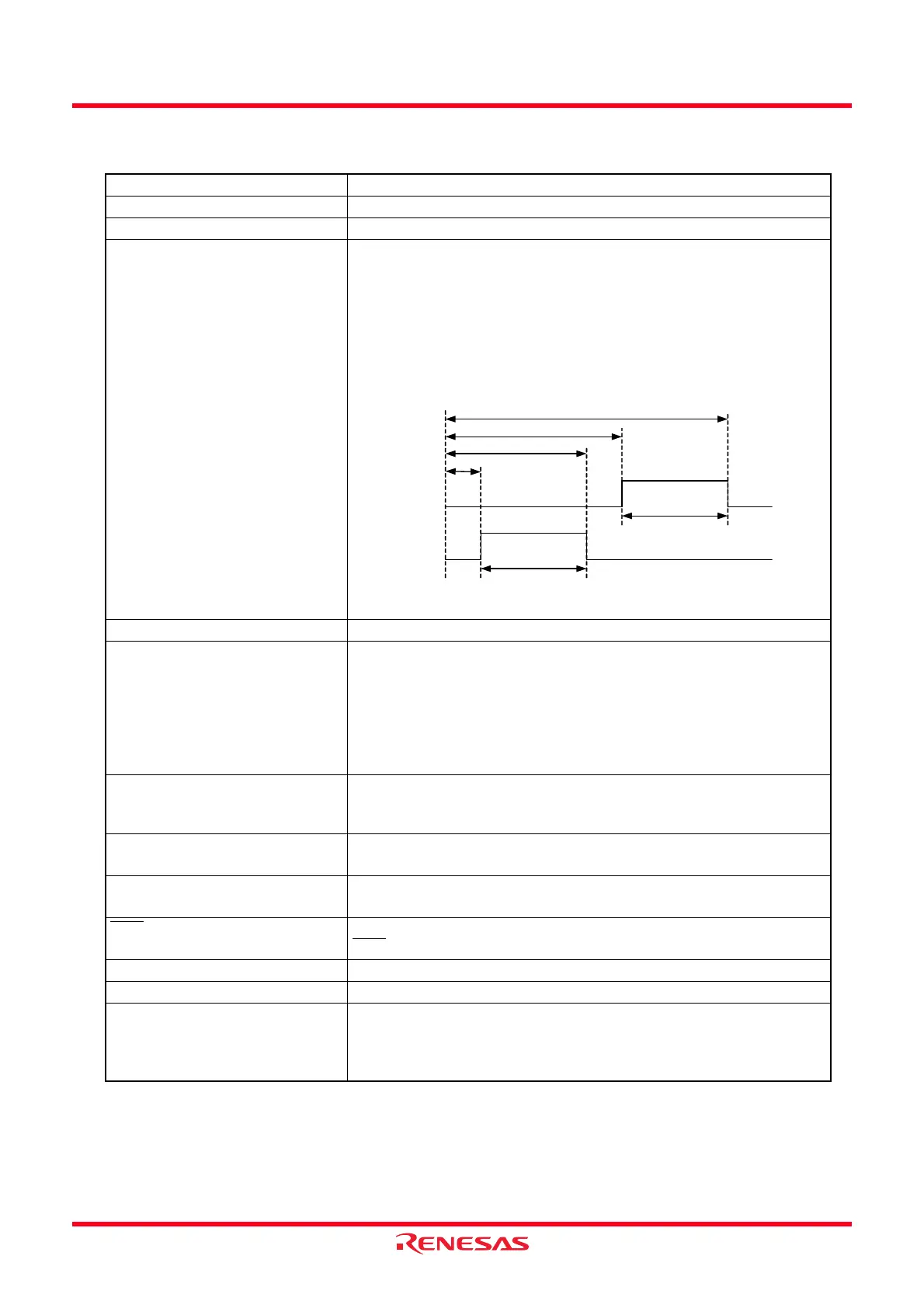
PWM Waveform PWM period: 1/fk × (m + 1)
Active level width of TRDIOA0 output: 1/fk × (m - n)
Active level width of TRDIOB0 output: 1/fk × (p - q)
fk: Frequency of count source
m: Setting value in the TRDGRA0 register
n: Setting value in the TRDGRA1 register
p: Setting value in the TRDGRB0 register
q: Setting value in the TRDGRB1 register
Count Start Condition Write 1 (count starts) to the TSTART0 bit in the TRDSTR register.
Count Stop Conditions • Write 0 (count stops) to the TSTART0 bit in the TRDSTR register
when the CSEL0 bit in the TRDSTR register is set to 1.
• The PWM output pin holds output level before the count stops
• When the CSEL0 bit in the TRDSTR register is set to 0, the count
stops at the compare match in the TRDGRA0 register.
• The PWM output pin holds level after output change by the compare
match.
Interrupt Request Generation
Timing
• Compare match (the content in the TRDi register matches with the
content in the TRDGRji register.)
• The TRD0 register overflows
TRDIOA0, TRDIOB0 Pin
Functions
PWM output
TRDIOC0, TRDIOD0, TRDIOA1
to TRDIOD1 Pin Functions
Programmable I/O port
INT0
Pin Function
Programmable I/O port, pulse output forced cutoff signal input or
INT0
interrupt input
Read from Timer The count value can be read by reading the TRD0 register.
Write to Timer The value can be written to the TRD0 register.
Selection Functions • Pulse output forced cutoff signal input (refer to 14.3.4 Pulse Output
Forced Cutoff)
• Select the active level every pin.
• Buffer operation (refer to 14.3.2 Buffer Operation)
m + 1
TRDIOA0 output
TRDIOB0 output
(When “H” is selected for the active level)
p - q
m - n
n + 1
p + 1
q + 1
 Loading...