R8C/20 Group, R8C/21 Group 14. Timers
Rev.2.00 Aug 27, 2008 Page 239 of 458
REJ09B0250-0200
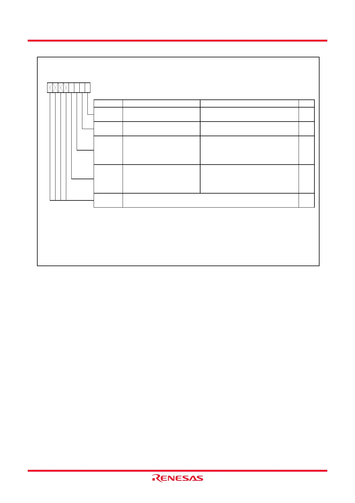
Figure 14.99 TRDSTR Register in PWM3 Mode
Timer RD Start Register
(1)
Symbol Address After Reset
TRDSTR
0137h 11111100b
Bit Symbol Bit Name Function RW
NOTES:
1.
2.
3.
4.
5.
—
(b7 - b4)
Nothing is assigned. If necessary, set to 0.
When read, the content is 1.
Set the TRDSTR register using the MOV instruction (do not use the bit handling instruction). Refer to
14.3.12.1
TRDSTR Re gis te r
of
Notes on Timer RD.
RW
TRD1 count operation select bit 0 : Count stops at the compare match
w ith the TRDGRA1 register
1 : Count continues at the compare
match w ith the TRDGRA1 register
—
TRD0 count operation select bit 0 : Count stops at the compare match
w ith the TRDGRA0 register
1 : Count continues at the compare
match w ith the TRDGRA0 register
CSEL0 RW
RW
TSTART1 RW
TRD1 count start flag
(5)
Set this bit to 0 (count stops) in PWM3
mode
(3)
TRD0 count start flag
(4)
0 : Count stops
(2)
1 : Count starts
b7 b6 b5 b4 b3 b2
CSEL1
b1 b0
0
TSTART0
When the CSEL0 bit is set to 1, w rite 0 to the TSTART0 bit.
When the CSEL1 bit is set to 1, w rite 0 to the TSTART1 bit.
When the CSEL0 bit is set to 0 and generating the compare match signal(TRDIOA0), this bit is set to 0 (count stops).
When the CSEL1 bit is set to 0 and generating the compare match signal(TRDIOA1), this bit is set to 0 (count stops).
 Loading...