R8C/20 Group, R8C/21 Group 14. Timers
Rev.2.00 Aug 27, 2008 Page 242 of 458
REJ09B0250-0200
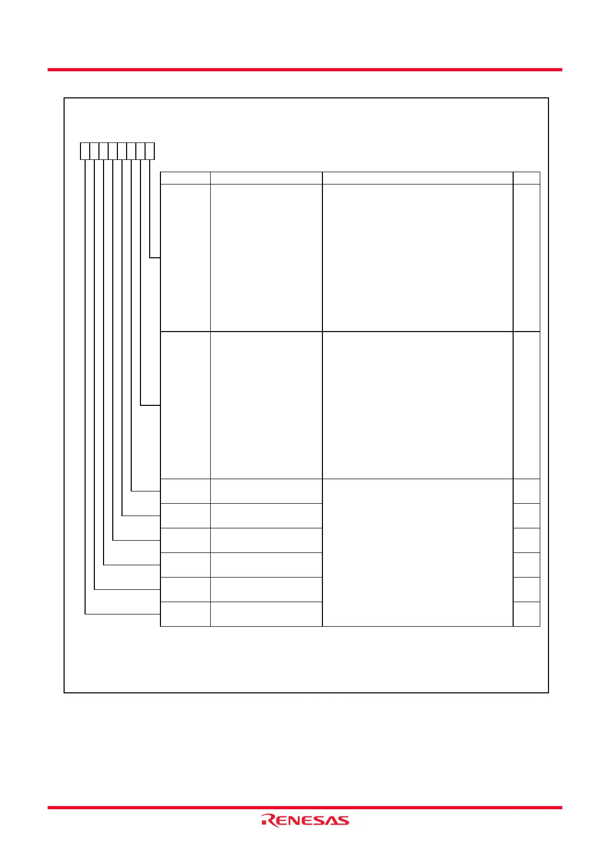
Figure 14.102 TRDOCR Register in PWM3 Mode
Timer RD Output Control Register
(1)
Symbol Address After Reset
TRDOCR
013Dh 00h
Bit Symbol Bit Name Function RW
NOTES:
1.
2. When the pin functions are w aveform output (refer to
Table 14.12
and
14.13
) and the TRDOCR register is set, the
initial output level is output.
TOA1
TOB1 RW
TRDIOD1 initial output level
selection bit
TRDIOB1 initial output level
selection bit
TOC1
TRDIOC1 initial output level
selection bit
This bit is disabled in PWM3 mode.TRDIOC0 initial output level
selection bit
Write to the TRDOCR register w hen both the TSTART0 and TSTART1 bits in the TRDSTR register are set to 0 (count
stops).
TOC0 RW
RW
TRDIOA1 initial output level
selection bit
RW
RW
TRDIOD0 initial output level
selection bit
TOD1 RW
RW
TOB0 RW
TRDIOA0 output level
selection bit
(2)
0 : Active level “H”,
initial output “L”,
output “H” by the compare match in the
TRDGRA1register,
output “L” by the compare match in the
TRDGRA0 register
1 : Active level “L”,
initial output “H”,
output “L” by the compare match in the
TRDGRA1register,
output “H” by the compare match in the
TRDGRA0 register
TRDIOB0 output level
selection bit
(2)
0 : Active level “H”,
initial output “L”,
output “H” by the compare match in the
TRDGRB1register,
output “L” by the compare match in the
TRDGRB0 register
1 : Active level “L”,
initial output “H”,
output “L” by the compare match in the
TRDGRB1register,
output “H” by the compare match in the
TRDGRB0 register
b7 b6 b5 b4 b3 b2
TOD0
b1 b0
TOA0
 Loading...