R8C/20 Group, R8C/21 Group 16. Clock Synchronous Serial Interface
Rev.2.00 Aug 27, 2008 Page 315 of 458
REJ09B0250-0200
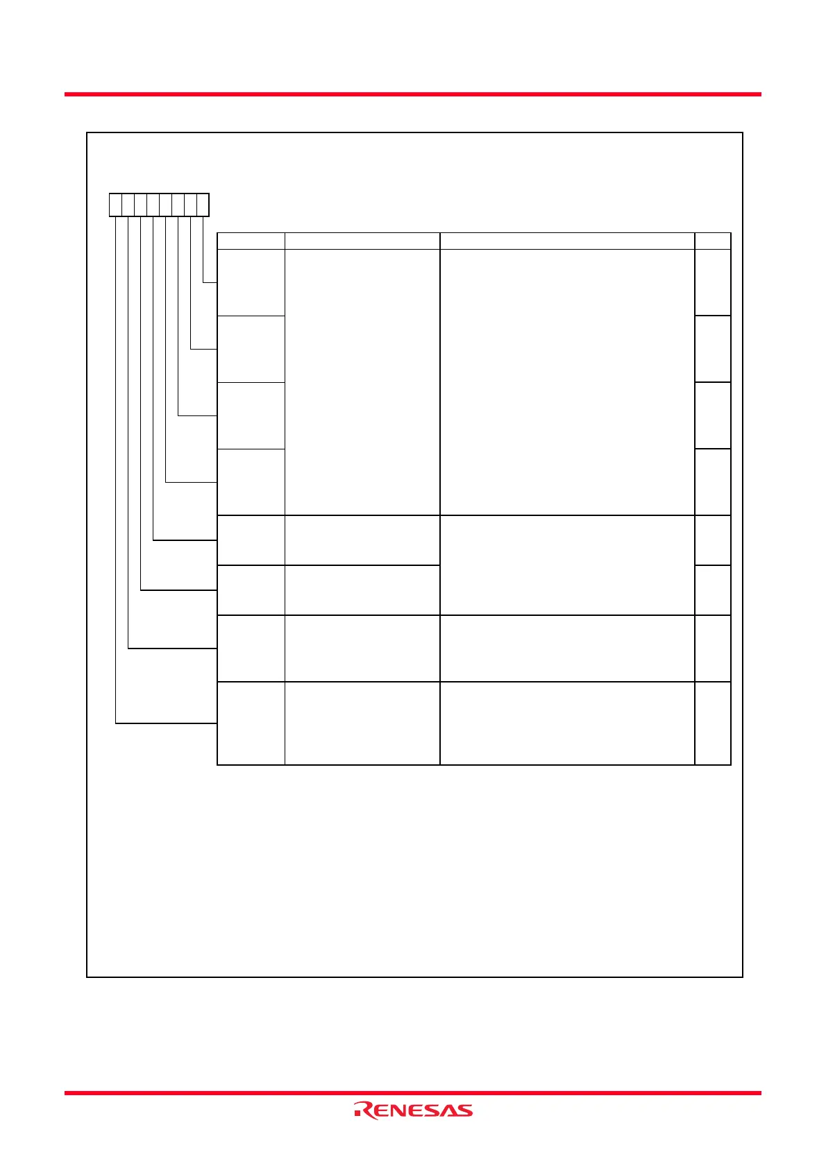
Figure 16.24 ICCR1 Register
IIC Bus Control Register 1
Symbol Address After Reset
ICCR1
00B8h 00h
Bit Symbol Bit Name Function RW
NOTES:
1.
2.
3.
4.
5.
6.
Master / slave select bit
(5,6)
In master mode w ith the
2
C bus format, w hen arbitration is lost, the MST and TRS bits are set to 0 and the IIC enters
slave receive mode.
When an overrun error occurs in master receive mode of the clock synchronous serial format, the MST bit is set to 0
and the IIC enters slave receive mode.
b0
Rew rite the TRS bit betw een the transfer frame.
RCVD
Receive disable bit After reading the ICDRR register w hile the TRS bit
is set to 0
0 : Maintains the follow ing receive operation
1 : Disables the follow ing receive operation
RW
b3 b2
RW
RW
b1b7 b6 b5 b4
CKS2
CKS3
CKS0
CKS1
RW
TRS
Transmit clock select bit 3 to
0
(1)
b3 b2 b1 b0
0 0 0 0 : f1/28
0 0 0 1 : f1/40
0 0 1 0 : f1/48
0 0 1 1 : f1/64
0 1 0 0 : f1/80
0 1 0 1 : f1/100
0 1 1 0 : f1/112
0 1 1 1 : f1/128
1 0 0 0 : f1/56
1 0 0 1 : f1/80
1 0 1 0 : f1/96
1 0 1 1 : f1/128
1 1 0 0 : f1/160
1 1 0 1 : f1/200
1 1 1 0 : f1/224
1 1 1 1 : f1/256
b5 b4
0 0 : Slave receive mode
(4)
0 1 : Slave transmit mode
1 0 : Master receive mode
1 1 : Master transmit mode
RW
MST RW
RW
Transfer / receive select
bit
(2,3,6)
In multimaster operation use the MOV instruction to set bits TRS and MST.
When the first 7 bits, after the start condition in slave receive mode, match w ith the slave address set in the SAR
register and the 8th bit is set to 1, the TRS bit is set to 1.
RWICE
I
2
C bus interface enable bit 0 : This module is halted
(SCL and SDA pins are set to port function)
1 : This module is enabled for transfer
operations
(SCL and SDA pins are bus drive state)
Set according to the necessary transfer rate in master mode. Refer to
Table 16.6 Transfer Rate Examples
for the
transfer rate. This bit is used for maintaining of the setup time in transmit mode. The time is 10Tcyc w hen the CKS3
bit is set to 0 and 20Tcyc w hen the CKS3 bit is set to 1. (1Tcyc = 1/f1(s))
 Loading...